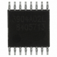
ICS83904AG-02LF IDT, Integrated Device Technology Inc, ICS83904AG-02LF Datasheet - Page 12

ICS83904AG-02LF
Manufacturer Part Number
ICS83904AG-02LF
Description
IC FANOUT BUFFER 1:4 16-TSSOP
Manufacturer
IDT, Integrated Device Technology Inc
Series
HiPerClockS™r
Type
Fanout Buffer (Distribution), Multiplexerr
Datasheet
1.ICS83904AG-02LF.pdf
(16 pages)
Specifications of ICS83904AG-02LF
Number Of Circuits
1
Ratio - Input:output
3:4
Differential - Input:output
No/No
Input
LVCMOS, LVTTL, Crystal
Output
LVCMOS, LVTTL
Frequency - Max
200MHz
Voltage - Supply
2.375 V ~ 3.465 V
Operating Temperature
0°C ~ 70°C
Mounting Type
Surface Mount
Package / Case
16-TSSOP
Frequency-max
200MHz
Lead Free Status / RoHS Status
Lead free / RoHS Compliant
Other names
800-1114
800-1114-5
800-1114
83904AG-02LF
800-1114-5
800-1114
83904AG-02LF
C
Figure 1 shows an example of ICS83904-02 crystal interface with
a parallel resonant crystal. The frequency accuracy can be fine
tuned by adjusting the C1 and C2 values. For a parallel crystal
with loading capacitance CL = 18pF, we suggest C1 = 15pF and
C2 = 15pF to start with. These values may be slightly fine tuned
further to optimize the frequency accuracy for different board
layouts. Slightly increasing the C1 and C2 values will slightly
reduce the frequency. Slightly decreasing the C1 and C2 values
will slightly increase the frequency. For the oscillator circuit below,
R1 can be used, but is not required. For new designs, it is
recommended that R1 not be used.
O
The XTAL_IN input can a single-ended LVCMOS signal through
an AC coupling capacitor. A general interface diagram is shown
in Figure 2A. The XTAL_OUT pin can be left floating. The maximum
amplitude of the input signal should not exceed 2V and the input
edge rate can be as slow as 10ns. This configuration requires
that the output impedance of the driver (Ro) plus the series
resistance (Rs) equals the transmission line impedance. In
addition, matched termination at the crystal input will attenuate
F
F
ICS83940AG-02 REVISION A SEPTEMBER 3, 2010
IGURE
IGURE
RYSTAL
VERDRIVING THE
3.3V
Driv er_LVCMOS
2A. G
2A. G
VCC=3.3V
I
NPUT
Ro ~ 7 Ohm
LVPECL
ENERAL
ENERAL
I
NTERFACE
RS
C
RYSTAL
D
D
IAGRAM FOR
IAGRAM FOR
43
Zo = 50 Ohm
Zo = 50 Ohm
Zo = 50 Ohm
I
NTERFACE
R2
50
LVCMOS D
LVPECL D
R1
100
R2
100
R1
50
R3
50
3.3V
C1
0.1uF
RIVER TO
RIVER TO
C1
0.1uF
XTAL_IN
XTAL_OUT
XTAL_IN
XTAL_OUT
XTAL I
XTAL I
Cry stal Input Interf ace
Cry stal Input Interf ace
NPUT
12
NPUT
the signal in half. This can be done in one of two ways. First, R1
and R2 in parallel should equal the transmission line impedance.
For most 50
also be accomplished by removing R1 and making R2 50 . By
overdring the crystal oscillator, the device will be functional, but
note, the device performance is guaranteed by using a quartz
crystal.
I
NTERFACE
I
NTERFACE
18pF Parallel Cry stal
X1
F
applications, R1 and R2 can be 100 . This can
IGURE
C2
15p
1. C
C1
15p
R1 (optional)
RYSTAL
0
2010 Integrated Device Technology, Inc.
I
NPUT
I
XTAL_IN
XTAL_OUT
NTERFACE


