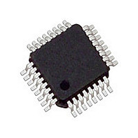
MPC9446FA IDT, Integrated Device Technology Inc, MPC9446FA Datasheet - Page 4

MPC9446FA
Manufacturer Part Number
MPC9446FA
Description
IC CLK DVDR FAN BUFF MUX 32LQFP
Manufacturer
IDT, Integrated Device Technology Inc
Type
Fanout Buffer (Distribution), Divider, Multiplexer , PLLr
Datasheet
1.MPC9446FA.pdf
(11 pages)
Specifications of MPC9446FA
Number Of Circuits
1
Ratio - Input:output
2:10
Differential - Input:output
No/No
Input
LVCMOS
Output
LVCMOS
Frequency - Max
250MHz
Voltage - Supply
2.375 V ~ 3.465 V
Operating Temperature
-40°C ~ 85°C
Mounting Type
Surface Mount
Package / Case
32-LQFP
Frequency-max
250MHz
Number Of Clock Inputs
2
Mode Of Operation
Single-Ended
Output Frequency
250MHz
Output Logic Level
LVCMOS
Operating Supply Voltage (min)
2.375V
Operating Supply Voltage (typ)
2.5/3.3V
Operating Supply Voltage (max)
3.465V
Package Type
TQFP
Operating Temp Range
-40C to 85C
Operating Temperature Classification
Industrial
Signal Type
LVCMOS
Mounting
Surface Mount
Pin Count
32
Quiescent Current
2mA
Lead Free Status / RoHS Status
Contains lead / RoHS non-compliant
Other names
800-2010
MPC9446FAIDT
MPC9446FAIDT
Available stocks
Company
Part Number
Manufacturer
Quantity
Price
Company:
Part Number:
MPC9446FA
Manufacturer:
IDT, Integrated Device Technology Inc
Quantity:
10 000
Part Number:
MPC9446FA
Manufacturer:
IDT
Quantity:
20 000
Company:
Part Number:
MPC9446FAR2
Manufacturer:
IDT, Integrated Device Technology Inc
Quantity:
10 000
IDT™ / ICS™ LVCMOS CLOCK FANOUT BUFFER
MPC9446
3.3V AND 2.5V LVCMOS CLOCK FANOUT BUFFER
Table 5. General Specifications
Table 6. DC Characteristics (V
Table 7. AC Characteristics (V
1. Input pull-up / pull-down resistors influence input current.
2. The MPC9446 is capable of driving 50 Ω transmission lines on the incident edge. Each output drives one 50 Ω parallel terminated
3. I
1. AC characteristics apply for parallel output termination of 50 Ω to V
2. The MPC9446 is functional up to an input and output clock frequency of 350 MHz and is characterized up to 250 MHz.
3. Violation of the 1.0 ns maximum input rise and fall time limit will affect the device propagation delay, device-to-device skew, reference input
4. Output pulse skew t
Symbol
Symbol
Symbol
t
t
I
t
PLZ, HZ
t
CCQ
PZL, LZ
Z
P, REF
t
HBM
t
f
sk(PP)
DC
C
V
t
t
SK(P)
V
V
MM
C
t
sk(O)
t
V
MAX
LU
V
transmission line to a termination voltage of V
PLH
PHL
pulse width, output duty cycle and maximum frequency specifications.
dependent: DC
I
OUT
f
r
r
CCQ
ref
IN
OH
, t
, t
TT
PD
OL
IH
IN
IL
Q
(3)
f
f
is the DC current consumption of the device with all outputs open and the input in its default state or open.
Output Termination Voltage
ESD Protection (Machine Model)
ESD Protection (Human Body Model)
Latch-Up Immunity
Power Dissipation Capacitance
Input Capacitance
Input High Voltage
Input Low Voltage
Input Current
Output High Voltage
Output Low Voltage
Output Impedance
Maximum Quiescent Supply Current
Input Frequency
Maximum Output Frequency
Reference Input Pulse Width
CCLK Input Rise/Fall Time
Propagation Delay
Output Disable Time
Output Enable Time
Output-to-Output Skew
Device-to-Device Skew
Output Pulse Skew
Output Duty Cycle
Output Rise/Fall Time
Q
= (0.5 ± t
Any output bank, same output divider
SK(P)
(1)
Characteristics
Characteristics
Characteristics
is the absolute difference of the propagation delay times: | t
Any output, Any output divider
SK(P)
(4)
CC
CC
•
f
OUT
= V
= V
CCLK0,1 to any Q
CCLK0,1 to any Q
). For example at f
CCA
CCA
Within one bank
= V
= V
TT
÷1 output
÷2 output
÷1 output
÷2 output
. Alternatively, the device drives up to two 50 Ω series terminated transmission lines.
CCB
CCB
= V
= V
OUT
CCC
CCC
= 125 MHz the output duty cycle limit is 50% ± 2.5%.
2000
–0.3
Min
200
200
= 3.3 V ± 5%, T
Min
= 3.3 V ± 5%, T
2.0
2.4
Min
1.4
2.2
2.2
0.1
47
45
0
0
0
TT
.
V
14 – 17
CC
Typ
Typ
4.0
10
Typ
2.8
2.8
50
50
A
A
÷ 2
= –40°C to +85°C)
= –40°C to +85°C)
PLH
– t
V
CC
PHL
250
250
Max
Max
0.55
0.30
1.0
200
Max
4.45
2.25
0.8
2.0
125
150
200
350
200
4.2
1.0
10
10
53
55
+ 0.3
(3)
(2)
(2)
|. Output duty cycle is frequency
(1)
MHz
MHz
MHz
Unit
Unit
Unit
4MPC9446 REV 4 NOVEMBER 28, 2007)
mA
mA
µA
pF
pF
ns
ns
ns
ns
ns
ns
ps
ps
ps
ns
ps
ns
Ω
%
%
V
V
V
V
V
V
V
V
Per output
LVCMOS
LVCMOS
V
I
I
I
All V
FSELx = 0
FSELx = 1
0.8 to 2.0 V
DC
DC
0.55 to 2.4 V
OH
OL
OL
IN
REF
REF
= 24 mA
= 12 mA
= GND or V
= –24 mA
CC
= 50%
= 25%–75%
Condition
Condition
Condition
Pins
(2)
(2)
IN
= VCC


