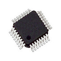
MPC9448FA IDT, Integrated Device Technology Inc, MPC9448FA Datasheet - Page 2

MPC9448FA
Manufacturer Part Number
MPC9448FA
Description
IC CLK FAN BUFF MUX 1:12 32LQFP
Manufacturer
IDT, Integrated Device Technology Inc
Type
Fanout Buffer (Distribution), Multiplexerr
Datasheet
1.MPC9448FA.pdf
(12 pages)
Specifications of MPC9448FA
Number Of Circuits
1
Ratio - Input:output
1:12
Differential - Input:output
Yes/No
Input
LVCMOS, LVPECL
Output
LVCMOS
Frequency - Max
350MHz
Voltage - Supply
2.375 V ~ 3.465 V
Operating Temperature
-40°C ~ 85°C
Mounting Type
Surface Mount
Package / Case
32-LQFP
Frequency-max
350MHz
Number Of Clock Inputs
2
Output Frequency
350MHz
Output Logic Level
LVCMOS
Operating Supply Voltage (min)
2.375V
Operating Supply Voltage (typ)
2.5/3.3V
Operating Supply Voltage (max)
3.465V
Package Type
TQFP
Operating Temp Range
-40C to 85C
Operating Temperature Classification
Industrial
Signal Type
LVCMOS/LVPECL
Mounting
Surface Mount
Pin Count
32
Quiescent Current
2mA
Lead Free Status / RoHS Status
Contains lead / RoHS non-compliant
Other names
800-2012
MPC9448FAIDT
MPC9448FAIDT
Available stocks
Company
Part Number
Manufacturer
Quantity
Price
Company:
Part Number:
MPC9448FA
Manufacturer:
IDT, Integrated Device Technology Inc
Quantity:
10 000
Company:
Part Number:
MPC9448FAR2
Manufacturer:
Freescale Semiconductor
Quantity:
10 000
IDT™ / ICS™ LVCMOS 1:12 CLOCK FANOUT BUFFER
MPC9448
3.3V/2.5V LVCMOS 1:12 CLOCK FANOUT BUFFER
Table 1. Function Table
Table 2. Pin Configurations
CLK_SEL
OE
CLK_STOP
PCLK, PCLK
CCLK
CLK_SEL
CLK_STOP
OE
Q0–11
GND
V
1. OE = 0 will high-impedance tristate all outputs independent on CLK_STOP.
CLK_STOP
CC
CLK_SEL
CCLK
PCLK
PCLK
Control
OE
Pin
V
V
V
CC
CC
CC
(All input resistors have a value of 25 kΩ)
Figure 1. Logic Diagram
Input
Input
Input
Input
Input
Output
Supply
Supply
V
CC
0
1
SYNC
Default
1
1
1
I/O
Stop
CLK
PECL differential input selected
Outputs disabled (high-impedance state)
Outputs synchronously stopped in logic low state
LVPECL
LVCMOS
LVCMOS
LVCMOS
LVCMOS
LVCMOS
Ground
V
CC
Type
Q9
Q0
Q1
Q2
Q3
Q4
Q5
Q6
Q7
Q8
Q10
Q11
2
GND
GND
Clock signal input
Alternative clock signal input
Clock input select
Clock output enable/disable
Output enable/disable (high-impedance tristate)
Clock outputs
Negative power supply (GND)
Positive power supply for I/O and core. All V
connected to the positive power supply for correct operation
V
V
Q3
Q2
Q1
Q0
CC
CC
0
Figure 2. 32-Lead Pinout (Top View)
25
26
27
28
29
30
31
32
24
1
(1)
23
2
22
3
MPC9448
Function
21
4
CCLK input selected
Outputs enabled
Outputs active
20
5
MPC9448
19
6
CC
18
7
pins must be
1
17
8
REV 6 JULY 11, 2006
16
15
14
13
12
11
10
9
GND
Q8
V
Q9
GND
Q10
V
Q11
CC
CC


