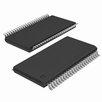
IDT5T9070PAGI IDT, Integrated Device Technology Inc, IDT5T9070PAGI Datasheet - Page 3

IDT5T9070PAGI
Manufacturer Part Number
IDT5T9070PAGI
Description
IC CLK BUFFER/DVR 1:10 48TSSOP
Manufacturer
IDT, Integrated Device Technology Inc
Series
TeraBuffer™ JRr
Type
Fanout Buffer (Distribution)r
Datasheet
1.IDT5T9070PAGI.pdf
(7 pages)
Specifications of IDT5T9070PAGI
Number Of Circuits
1
Ratio - Input:output
1:10
Differential - Input:output
No/No
Input
LVTTL
Output
LVTTL
Frequency - Max
200MHz
Voltage - Supply
2.3 V ~ 2.7 V
Operating Temperature
-40°C ~ 85°C
Mounting Type
Surface Mount
Package / Case
48-TSSOP
Frequency-max
200MHz
Number Of Outputs
10
Operating Supply Voltage (max)
2.7V
Operating Temp Range
-40C to 85C
Propagation Delay Time
3.5ns
Operating Supply Voltage (min)
2.3V
Mounting
Surface Mount
Pin Count
48
Operating Supply Voltage (typ)
2.5V
Package Type
TSSOP
Quiescent Current
2mA
Input Frequency
200MHz
Operating Temperature Classification
Industrial
Lead Free Status / RoHS Status
Lead free / RoHS Compliant
Other names
5T9070PAGI
800-1984-5
IDT5T9070PAGI
800-1984-5
IDT5T9070PAGI
Available stocks
Company
Part Number
Manufacturer
Quantity
Price
Company:
Part Number:
IDT5T9070PAGI
Manufacturer:
ADI
Quantity:
184
Part Number:
IDT5T9070PAGI
Manufacturer:
IDT
Quantity:
20 000
PIN DESCRIPTION
NOTE:
1. Because the gate controls are asynchronous, runt pulses are possible. It is the user's responsibility to either time the gate control signals to minimize the possibility of runt
DC ELECTRICAL CHARACTERISTICS OVER OPERATING RANGE
NOTES:
1. See RECOMMENDED OPERATING RANGE table.
2. Voltage required to maintain a logic HIGH.
3. Voltage required to maintain a logic LOW.
4. Typical values are at V
Symbol
IDT5T9070
2.5V SINGLE DATA RATE 1:10 CLOCK BUFFER TERABUFFER JR.
GND
pulses or be able to tolerate them in down stream circuitry.
Symbol
V
G1
G2
GL
Qn
A
V
DD
V
V
V
V
V
I
I
IH
IL
OH
OL
IK
IN
IH
IL
I/O
O
I
I
I
I
Input HIGH Current
Input LOW Current
Clamp Diode Voltage
DC Input Voltage
DC Input HIGH
DC Input LOW
Output HIGH Voltage
Output LOW Voltage
DD
LVTTL
LVTTL
LVTTL
LVTTL
LVTTL
Type
PWR
PWR
Parameter
= 2.5V, +25°C ambient.
(3)
(2)
Description
Clock input
Gate for outputs Q
nously disabled to the level designated by GL
Gate for outputs Q
nously disabled to the level designated by GL
Specifies output disable level. If HIGH, the outputs disable HIGH. If LOW, the outputs disable LOW.
Clock outputs
Power supply for the device core, inputs, and outputs
Power supply return for power
1
6
through Q
through Q
V
V
V
I
I
I
I
OH
OH
OL
OL
DD
DD
DD
= 12mA
= 100μA
= -100μA
= -12mA
= 2.3V, I
= 2.7V
= 2.7V
5
10
. When G1 is LOW, these outputs are enabled. When G1 is HIGH, these outputs are asynchro-
. When G2 is LOW, these outputs are enabled. When G2 is HIGH, these outputs are asynchro-
Test Conditions
IN
= -18mA
3
(1)
(1)
.
.
V
V
I
I
= V
= GND/V
DD
/GND
DD
V
V
DD
DD
Min.
- 0.3
1.7
—
—
—
—
—
—
- 0.1
- 0.4
INDUSTRIAL TEMPERATURE RANGE
Typ.
- 0.7
—
—
(4)
(1)
+3.6
Max
- 1.2
0.7
0.4
0.1
±5
±5
—
—
—
Unit
μA
V
V
V
V
V
V
V
V


