IDT5T30553DCGI IDT, Integrated Device Technology Inc, IDT5T30553DCGI Datasheet - Page 2
IDT5T30553DCGI
Manufacturer Part Number
IDT5T30553DCGI
Description
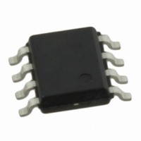
IC CLK BUFFER/DVR 1:4 8SOIC
Manufacturer
IDT, Integrated Device Technology Inc
Type
Fanout Buffer (Distribution)r
Datasheet
1.IDT5T30553DCGI.pdf
(8 pages)
Specifications of IDT5T30553DCGI
Number Of Circuits
1
Ratio - Input:output
1:4
Differential - Input:output
No/No
Input
Clock
Output
Clock
Frequency - Max
200MHz
Voltage - Supply
2.375 V ~ 3.45 V
Operating Temperature
-40°C ~ 85°C
Mounting Type
Surface Mount
Package / Case
8-SOIC (3.9mm Width)
Frequency-max
200MHz
Number Of Outputs
4
Operating Supply Voltage (max)
3.45V
Operating Temp Range
-40C to 85C
Propagation Delay Time
5ns
Operating Supply Voltage (min)
2.375V
Mounting
Surface Mount
Pin Count
8
Operating Supply Voltage (typ)
2.5/3.3V
Package Type
SOIC N
Input Frequency
200MHz
Operating Temperature Classification
Industrial
Lead Free Status / RoHS Status
Lead free / RoHS Compliant
Other names
800-1919-5


Pin Assignment
Pin Descriptions
External Components
IDT™ LOW SKEW 1 TO 4 CLOCK BUFFER
Number
IDT5T30553
LOW SKEW 1 TO 4 CLOCK BUFFER
Pin
1
2
3
4
5
6
7
8
A minimum number of external components are required for proper operation. A decoupling capacitor of 0.01 µF
should be connected between VDD on pin 1 and GND on pin 4, as close to the device as possible. A 33
terminating resistor may be used on each clock output if the trace is longer than 1 inch.
To achieve the low output skew that the IDT5T30553 is capable of, careful attention must be paid to board layout.
Essentially, all four outputs must have identical terminations, identical loads and identical trace geometries. If they
do not, the output skew will be degraded. For example, using a 30 series termination on one output (with 33 on
the others) will cause at least 15 ps of skew.
GN D
V D D
Q0
Q1
Name
GND
ICLK
VDD
Pin
OE
Q0
Q1
Q2
Q3
1
2
3
4
Output
Output
Output
Output
Power
Power
Type
Input
Input
8 - p i n S OI C
Pin
Clock output 0.
Clock output 1.
Clock input.
Clock Output 2.
Clock Output 3.
Output Enable. Tri-states outputs when low. Connect to VDD for normal operation.
Connect to +2.5 V or +3.3 V.
Connect to ground.
8
7
6
5
O E
Q 3
Q 2
I CL K
2
Pin Description
IDT5T30553
FAN OUT BUFFER
REV C 090209
series
Related parts for IDT5T30553DCGI
Image
Part Number
Description
Manufacturer
Datasheet
Request
R

Part Number:
Description:
TRANSLATION DEVICE DPI 80-PQFP
Manufacturer:
IDT, Integrated Device Technology Inc
Datasheet:
Part Number:
Description:
IDT PART
Manufacturer:
IDT, Integrated Device Technology Inc
Datasheet:
Part Number:
Description:
IC LIU T1/E1/J1 OCTAL 256PBGA
Manufacturer:
IDT, Integrated Device Technology Inc
Datasheet:

Part Number:
Description:
IC FREQ TIMING GENERATOR 28TSSOP
Manufacturer:
IDT, Integrated Device Technology Inc
Datasheet:
Part Number:
Description:
IC CLK DVR PLL 1:10 40VFQFPN
Manufacturer:
IDT, Integrated Device Technology Inc
Datasheet:
Part Number:
Description:
IC CLK FANOUT BUFFER 1:18 32LQFP
Manufacturer:
IDT, Integrated Device Technology Inc
Datasheet:
Part Number:
Description:
IC CLK FANOUT BUFFER 1:18 32LQFP
Manufacturer:
IDT, Integrated Device Technology Inc
Datasheet:
Part Number:
Description:
IC CK505 VREG/RES 56TSSOP
Manufacturer:
IDT, Integrated Device Technology Inc
Datasheet:

Part Number:
Description:
IC SDRAM CLK DVR 1:10 48-TSSOP
Manufacturer:
IDT, Integrated Device Technology Inc
Datasheet:

Part Number:
Description:
IC CLK DVR PLL 1:10 48TSSOP
Manufacturer:
IDT, Integrated Device Technology Inc
Datasheet:
Part Number:
Description:
IC FLEXPC CLK PROGR P4 56-TSSOP
Manufacturer:
IDT, Integrated Device Technology Inc
Datasheet:
Part Number:
Description:
IC FLEXPC CLK PROGR P4 56-TSSOP
Manufacturer:
IDT, Integrated Device Technology Inc
Datasheet:
Part Number:
Description:
IC FLEXPC CLK PROGR P4 56-SSOP
Manufacturer:
IDT, Integrated Device Technology Inc
Datasheet:

Part Number:
Description:
IC PLL CLK DRIVER 2.5V 28-TSSOP
Manufacturer:
IDT, Integrated Device Technology Inc
Datasheet:
Part Number:
Description:
IC CLOCK DRIVER 2.5V 24-TSSOP
Manufacturer:
IDT, Integrated Device Technology Inc
Datasheet: