IDT5V2310PGGI IDT, Integrated Device Technology Inc, IDT5V2310PGGI Datasheet
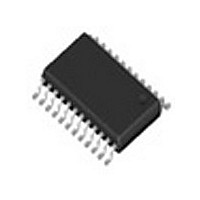
IC CLK BUFFER/DVR 1:10 24TSSOP

IDT5V2310PGGI

Manufacturer Part Number
IDT5V2310PGGI
Description
IC CLK BUFFER/DVR 1:10 24TSSOP
Manufacturer
IDT, Integrated Device Technology Inc
Type
Fanout Buffer (Distribution)r
Datasheets

Specifications of IDT5V2310PGGI

Number Of Circuits
1
Ratio - Input:output
1:10
Differential - Input:output
No/No
Input
LVTTL
Output
LVTTL
Frequency - Max
200MHz
Voltage - Supply
2.3 V ~ 3.6 V
Operating Temperature
-40°C ~ 85°C
Mounting Type
Surface Mount
Package / Case
24-TSSOP
Frequency-max
200MHz
Number Of Outputs
10
Operating Supply Voltage (max)
3.6V
Operating Temp Range
-40C to 85C
Propagation Delay Time
3.5ns
Operating Supply Voltage (min)
2.3V
Mounting
Surface Mount
Pin Count
24
Operating Supply Voltage (typ)
2.5/3.3V
Package Type
TSSOP
Input Frequency
200MHz
Operating Temperature Classification
Industrial
Lead Free Status / RoHS Status
Lead free / RoHS Compliant
Other names
5V2310PGGI
800-1990-5
IDT5V2310PGGI

Available stocks

Company
Part Number
Manufacturer
Quantity
Price
Part Number:
IDT5V2310PGGI
Manufacturer:
IDT
Quantity:
562
Part Number:
IDT5V2310PGGI
Manufacturer:
IDT
Quantity:
588
Part Number:
IDT5V2310PGGI
Manufacturer:
IDT
Quantity:
20 000
Part Number:
IDT5V2310PGGI8
Manufacturer:
IDT
Quantity:
20 000
FEATURES:
• High performance 1:10 clock driver for general purpose
• Operates up to 200MHz at V
• Pin-to-pin skew < 100ps
• V
• Output enable glitch suppression
• Distributes one clock input to two banks of five outputs
• 25Ω Ω Ω Ω Ω on-chip series dampening resistors
• Available in TSSOP and VFQFPN packages
FUNCTIONAL BLOCK DIAGRAM
The IDT logo is a registered trademark of Integrated Device Technology, Inc.
INDUSTRIAL TEMPERATURE RANGE
IDT5V2310
2.5V TO 3.3V HIGH PERFORMANCE CLOCK BUFFER
c
applications
DD
2004
range: 2.3V to 3.6V
Integrated Device Technology, Inc.
DD
= 3.3V
CLK
1G
2G
2.5V TO 3.3V HIGH
PERFORMANCE CLOCK
BUFFER
11
13
24
LOGIC CONTROL
LOGIC CONTROL
1
DESCRIPTION:
operates up to 200MHz. Two banks of five outputs each provide low skew
copies of CLK. Through the use of control pins 1G and 2G, the outputs of
banks 1Y(0:4) and 2Y(0:4) can be placed in a low state regardless of CLK
input. The device operates in 2.5V and 3.3V environments. The built-in
output enable glitch suppression ensures a synchronized output enable
sequence to distribute full period clock signals.
The IDT5V2310 is a high performance, low skew clock buffer that
The IDT5V2310 is characterized for operation from -40°C to +85°C.
25
25
25
25
25
25
25
25
25
25
3
4
5
8
9
21
20
17
16
12
1
1
1
1
1
2
2
2
2
2
Y
Y
Y
Y
Y
Y
Y
Y
Y
Y
0
1
2
3
4
0
1
2
3
4
INDUSTRIAL TEMPERATURE RANGE
IDT5V2310
MAY 2010
DSC 6173/25

Related parts for IDT5V2310PGGI

IDT5V2310PGGI Summary of contents

Page 1

IDT5V2310 2.5V TO 3.3V HIGH PERFORMANCE CLOCK BUFFER FEATURES: • High performance 1:10 clock driver for general purpose applications • Operates up to 200MHz 3.3V DD • Pin-to-pin skew < 100ps • V range: 2.3V to 3.6V ...

Page 2

IDT5V2310 2.5V TO 3.3V HIGH PERFORMANCE CLOCK BUFFER PIN CONFIGURATION GND GND 6 7 GND ...

Page 3

IDT5V2310 2.5V TO 3.3V HIGH PERFORMANCE CLOCK BUFFER PIN DESCRIPTION TERMINAL Symbol I Output Enable Control for input clock (CLK). If this pin is logic LOW, the 2G I Output Enable Control for input clock (CLK). If this ...

Page 4

IDT5V2310 2.5V TO 3.3V HIGH PERFORMANCE CLOCK BUFFER DC ELECTRICAL CHARACTERISTICS - V Symbol Parameter V HIGH level Output Voltage OH V LOW level Output Voltage OL I HIGH level Output Current OH I LOW level Output Current OL NOTE: ...

Page 5

IDT5V2310 2.5V TO 3.3V HIGH PERFORMANCE CLOCK BUFFER SWITCHING CHARACTERISTICS OVER OPERATING RANGE - V = 3.3V ± 0.3V (1) DD Symbol Parameter t CLK to Yx PLH t PHL ( Output Skew ...

Page 6

IDT5V2310 2.5V TO 3.3V HIGH PERFORMANCE CLOCK BUFFER OUTPUT ENABLE GLITCH SUPPRESSION CIRCUIT The purpose of the glitch suppression circuitry is to ensure the output enable sequence is synchronized with the clock input such that the output buffer will be ...

Page 7

IDT5V2310 2.5V TO 3.3V HIGH PERFORMANCE CLOCK BUFFER TEST CIRCUITS AND WAVEFORMS FROM OUTPUT NOTES All input pulses are supplied by generators having the following characteristics: PRR ≤ 200MHz; Z CLK Yx CLK Any Y Any Y ...

Page 8

IDT5V2310 2.5V TO 3.3V HIGH PERFORMANCE CLOCK BUFFER RECOMMENDED LANDING PATTERN NOTE: All dimensions are in millimeters. INDUSTRIAL TEMPERATURE RANGE NR 20 pin 8 ...

Page 9

IDT5V2310 2.5V TO 3.3V HIGH PERFORMANCE CLOCK BUFFER ORDERING INFORMATION 5V2310PGGI Tubes 24-pin TSSOP 5V2310PGGI8 Tape & Reel 24-pin TSSOP 5V2310NRGI Tubes 20-pin VFQFPN 5V2310NRGI8 Tape & Reel 20-pin VFQFPN CORPORATE HEADQUARTERS 6024 Silver Creek Valley Road San Jose, CA ...

Related keywords