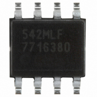
ICS542MLF IDT, Integrated Device Technology Inc, ICS542MLF Datasheet - Page 2

ICS542MLF
Manufacturer Part Number
ICS542MLF
Description
IC CLK DIVIDER 156MHZ 8-SOIC
Manufacturer
IDT, Integrated Device Technology Inc
Type
Fanout Buffer (Distribution), Dividerr
Datasheet
1.ICS542MLF.pdf
(6 pages)
Specifications of ICS542MLF
Number Of Circuits
1
Ratio - Input:output
1:2
Differential - Input:output
No/No
Input
CMOS
Output
3-State, CMOS
Frequency - Max
156MHz
Voltage - Supply
3 V ~ 5.5 V
Operating Temperature
0°C ~ 70°C
Mounting Type
Surface Mount
Package / Case
8-SOIC
Frequency-max
156MHz
Number Of Outputs
2
Operating Supply Voltage (max)
5.5V
Operating Temp Range
0C to 70C
Propagation Delay Time
15ns
Operating Supply Voltage (min)
3V
Mounting
Surface Mount
Pin Count
8
Operating Supply Voltage (typ)
3.3/5V
Package Type
SOIC N
Input Frequency
156MHz
Duty Cycle
55%
Operating Temperature Classification
Commercial
Lead Free Status / RoHS Status
Lead free / RoHS Compliant
Other names
542MLF
800-1053
800-1053-5
800-1053
800-1053
800-1053-5
800-1053
Available stocks
Company
Part Number
Manufacturer
Quantity
Price
Company:
Part Number:
ICS542MLF
Manufacturer:
IDT
Quantity:
5 299
Part Number:
ICS542MLF
Manufacturer:
ICS
Quantity:
20 000
Company:
Part Number:
ICS542MLFT
Manufacturer:
IDT
Quantity:
472
Part Number:
ICS542MLFT
Manufacturer:
IDT
Quantity:
20 000
Pin Assignment
Pin Descriptions
External Components
Series Termination Resistor
Clock output traces over one inch should use series
termination. To series terminate a 50 trace (a commonly
used trace impedance), place a 33 resistor in series with
the clock line, as close to the clock output pin as possible.
The nominal impedance of the clock output is 20 .
Decoupling Capacitor
As with any high-performance mixed-signal IC, the ICS542
must be isolated from system power supply noise to perform
optimally.
A decoupling capacitor of 0.01µF must be connected
between VDD and the PCB ground plane.
IDT™ / ICS™ CLOCK DIVIDER
ICS542
CLOCK DIVIDER
I CLK
GND
Number
VDD
S0
Pin
1
2
3
4
5
6
7
8
8-pin (150 mil) SOIC
1
2
3
4
Name
CLK/2
ICLK
GND
VDD
CLK
Pin
OE
S0
S1
8
7
6
5
Output
Output
Power
Power
Type
Input
Input
Input
Pin
XI
CLK
CLK/ 2
OE
S1
Clock input.
Connect to +3.3 V or +5 V.
Connect to ground.
Select 0 for output clock. Connect to GND or VDD, per decoding table above.
Internal pull-up resistor.
Select 1 for output clock. Connect to GND or VDD, per decoding table above.
Internal pull-up resistor.
Output Enable. Tri-states both output clocks when low. Internal pull-up
resistor.
Clock output per table above. Low skew divide by two of pin 8 clock.
Clock output per table above.
2
Clock Decoding Table
0 = connect directly to ground
1 = connect directly to VDD
PCB Layout Recommendations
For optimum device performance and lowest output phase
noise, the following guidelines should be observed.
1) The 0.01µF decoupling capacitor should be mounted on
the component side of the board as close to the VDD pin as
possible. No vias should be used between decoupling
capacitor and VDD pin. The PCB trace to VDD pin should
be kept as short as possible, as should the PCB trace to the
ground via. Distance of the ferrite bead and bulk decoupling
from the device is less critical.
2) To minimize EMI, the 33 series termination resistor (if
needed) should be placed close to the clock output.
3) An optimum layout is one with all components on the
S1
0
0
1
1
S0
0
1
0
1
Pin Description
Input/6
Input/8
Input/2
CLK
Power Down All
ICS542
Input/12
Input/16
CLK/2
Input/4
CLOCK DIVIDER
REV J 051310


