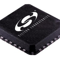
SI5017-BM Silicon Laboratories Inc, SI5017-BM Datasheet - Page 24

SI5017-BM
Manufacturer Part Number
SI5017-BM
Description
IC CLOCK/DATA RECOVERY 28MLP
Manufacturer
Silicon Laboratories Inc
Type
Clock and Data Recovery (CDR)r
Specifications of SI5017-BM
Input
Differential
Output
CML
Frequency - Max
2.7GHz
Voltage - Supply
3.135 V ~ 3.465 V
Operating Temperature
-40°C ~ 85°C
Mounting Type
Surface Mount
Package / Case
28-VQFN Exposed Pad, 28-HVQFN, 28-SQFN, 28-DHVQFN
Frequency-max
2.7GHz
For Use With/related Products
Si5017
Lead Free Status / RoHS Status
Contains lead / RoHS non-compliant
Lead Free Status / RoHS Status
Lead free / RoHS Compliant, Contains lead / RoHS non-compliant
Other names
336-1124
Si5017
Document Change List
Revision 0.1 to Revision 1.0
!
!
!
!
!
!
!
Revision 1.0 to Revision 1.1
!
Revision 1.1 to Revision 1.2
!
!
!
!
24
Added Figure 4, “PLL Acquisition Time,” on page 6.
Table 2 on page 7
"
"
"
"
"
"
Table 3 on page 8
"
"
"
"
Table 4 on page 9
"
"
"
"
"
Removed “Hysteresis Dependency” Figure.
Added Figure 7, “LOS Signal Hysteresis,” on page
13.
Corrected error: Table 8 on page 19—changed
description for LOS_LVL from “LOS is disabled when
the voltage applied is less than 500 mV” to “LOS is
disabled when the voltage applied is less than
1.0 V.”
Corrected “Revision 0.1 to Revision 1.0” Change
List.
Added Figure 5, “LOS Response Time,” on page 6.
Updated Table 2 on page 7
"
updated values.
"
updated values.
Table 3 on page 8.
"
"
Updated Table 8 on page 19
"
Added “Output Common Mode Voltage (CLKOUT)” with
(REFCLK)
(reference clock applied)
(reference-less operation)
goes out of Lock
goes into Lock
Changed “clock input” to “DIN inputs” for Loss-of-Signal.
Added FEC (2.7 GHz) Supply Current
Updated values: Supply Current
Added FEC (2.7 GHz) Power Dissipation
Updated values: Power Dissipation
Updated values: Common Mode Input Voltage
Updated values: Output Common Mode Voltage
Added separate Output Clock Rise Time
Added separate Output Clock Fall Time
Updated values: Output Clock Rise Time
Updated values: Output Clock Fall Time
Updated values: Jitter Tolerance (OC-48) for f = 1 MHz
Updated values: Acquisition Time
Updated values: Acquisition Time
Updated values: Freq Difference at which Receive PLL
Updated values: Freq Difference at which Receive PLL
Added “Output Common Mode Voltage (DOUT)” with
Added “Output Clock Duty Cycle”
Added “Loss-of-Signal Response Time”
Rev. 1.2
!
!
Updated Figure 16, “28-Lead Micro Leaded Package
(MLP),” on page 23.
Updated Table 9, “Package Diagram Dimensions,”
on page 23.
"
"
Changed dimension A.
Changed dimension E2.


