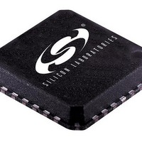
SI5017-BM Silicon Laboratories Inc, SI5017-BM Datasheet - Page 13

SI5017-BM
Manufacturer Part Number
SI5017-BM
Description
IC CLOCK/DATA RECOVERY 28MLP
Manufacturer
Silicon Laboratories Inc
Type
Clock and Data Recovery (CDR)r
Specifications of SI5017-BM
Input
Differential
Output
CML
Frequency - Max
2.7GHz
Voltage - Supply
3.135 V ~ 3.465 V
Operating Temperature
-40°C ~ 85°C
Mounting Type
Surface Mount
Package / Case
28-VQFN Exposed Pad, 28-HVQFN, 28-SQFN, 28-DHVQFN
Frequency-max
2.7GHz
For Use With/related Products
Si5017
Lead Free Status / RoHS Status
Contains lead / RoHS non-compliant
Lead Free Status / RoHS Status
Lead free / RoHS Compliant, Contains lead / RoHS non-compliant
Other names
336-1124
Lock Detect
The Si5017 provides lock-detect circuitry that indicates
whether the PLL has achieved frequency lock with the
incoming data. The operation of the lock-detector
depends on the reference clock option used.
When an external reference clock is provided, the circuit
compares the frequency of a divided-down version of
the recovered clock with the frequency of the applied
reference clock (REFCLK). If the recovered clock
frequency deviates from that of the reference clock by
the amount specified in Table 4 on page 9, the PLL is
declared out of lock, and the loss-of-lock (LOL) pin is
asserted. In this state, the PLL will periodically try to
reacquire lock with the incoming data stream. During
reacquisition, the recovered clock frequency (CLKOUT)
drifts over a ±600 ppm range relative to the applied
reference clock and the LOL output alarm may toggle
until the PLL has reacquired frequency lock. Due to the
low noise and stability of the DSPLL, there is the
possibility that the PLL will not drift enough to render an
out-of-lock condition, even if the data is removed from
inputs.
In applications requiring a more stable output clock
during out-of-lock conditions, the lock-to-reference
(LTR) input can be used to force the PLL to lock to the
externally supplied reference.
In the absence of an external reference, the lock detect
circuitry uses a data quality measure to determine when
frequency lock has been lost with the incoming data
stream. During reacquisition, CLKOUT may vary by
approximately ±10% from the nominal data rate.
Lock-to-Reference
The LTR input is used to force a stable output clock
when an alarm condition, like LOS, exists. In typical
applications, the LOS output is tied to the LTR input to
force a stable output clock when the input data signal is
lost. When LTR is asserted, the DSPLL is prevented
from acquiring the data signal present on DIN. The
operation of the LTR control input depends on which
reference clocking mode is used.
When an external reference clock is present, assertion
Table 7. Typical REFCLK Frequencies
SONET/SDH
155.52 MHz 166.63 MHz
19.44 MHz
77.76 MHz
OC-48 with
15/14 FEC
20.83 MHz
83.31 MHz
Ratio of VCO
to REFCLK
128
32
16
Rev. 1.2
of LTR forces the DSPLL to lock CLKOUT to the
provided reference. If no external reference clock is
used, LTR forces the DSPLL to hold the digital
frequency control input to the VCO at the last value.
This produces a stable output clock as long as supply
and temperature are constant.
Loss-of-Signal
The Si5017 indicates a loss-of-signal condition on the
LOS output pin when the input peak-to-peak signal level
on DIN falls below an externally controlled threshold.
The LOS threshold range is specified in Table 3 and is
set by applying a voltage on the LOS_LVL pin. The
graph in Figure 6 illustrates the LOS_LVL mapping to
the LOS threshold. The LOS output is asserted when
the input signal drops below the programmed peak-to-
peak value. If desired, the LOS function may be
disabled by grounding LOS_LVL or by adjusting
LOS_LVL to be less than 1 V.
Set LOS
40 mV
30 mV
15 mV
Level
0 mV
Figure 7. LOS Signal Hysteresis
R1
R2
0 V
Figure 6. LOS_LVL Mapping
10k
3
1.00 V
LOS_LVL
LOS_LVL (V)
Si5017
CDR
1.50 V
LOS
1.875 V
9
Si5017
40 mV/V
LOS Alarm
2.25 V
2.5 V
13


