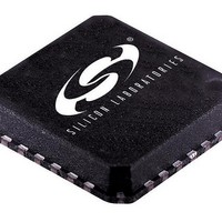
SI5017-BM Silicon Laboratories Inc, SI5017-BM Datasheet - Page 14

SI5017-BM
Manufacturer Part Number
SI5017-BM
Description
IC CLOCK/DATA RECOVERY 28MLP
Manufacturer
Silicon Laboratories Inc
Type
Clock and Data Recovery (CDR)r
Specifications of SI5017-BM
Input
Differential
Output
CML
Frequency - Max
2.7GHz
Voltage - Supply
3.135 V ~ 3.465 V
Operating Temperature
-40°C ~ 85°C
Mounting Type
Surface Mount
Package / Case
28-VQFN Exposed Pad, 28-HVQFN, 28-SQFN, 28-DHVQFN
Frequency-max
2.7GHz
For Use With/related Products
Si5017
Lead Free Status / RoHS Status
Contains lead / RoHS non-compliant
Lead Free Status / RoHS Status
Lead free / RoHS Compliant, Contains lead / RoHS non-compliant
Other names
336-1124
Si5017
In many applications it is desirable to produce a fixed
amount of signal hysteresis for an alarm indicator such
as LOS, since a marginal data input signal could cause
intermittent toggling, leading to false alarm status.
When it is anticipated that very low-level DIN signals will
be encountered, the introduction of an adequate
amount of LOS hysteresis is recommended to minimize
any undesirable LOS signal toggling. Figure 7 illustrates
a simple circuit that may be used to set a fixed level of
LOS signal hysteresis for the Si5017 CDR. The value of
R1 may be chosen to provide a range of hysteresis from
3 to 8 dB where a nominal value of 800 Ω adjusts the
hysteresis level to approximately 6 dB. Use a value of
500 Ω or 1000 Ω for R1 to provide 3 dB or 8 dB of
hysteresis, respectively.
Hysteresis is defined as the ratio of the LOS deassert
level (LOSD) and the LOS assert level (LOSA). The
hysteresis in decibels is calculated as 20log(LOSD/
LOSA).
Bit-Error-Rate (BER) Detection
The Si5017 uses a proprietary Silicon Laboratories®
algorithm to generate a bit-error-rate (BER) alarm on
the BER_ALM pin if the observed BER is greater than a
user programmable threshold. Bit error detection relies
on the input data edge timing; edges occurring outside
of the expected event window are counted as bit errors.
The BER threshold is programmed by applying a
voltage to the BER_LVL pin between 500 mV and
2.25 V corresponding to a BER of approximately 10
and 10
BER_LVL maps to the BER as follows: log10(BER) =
(4 x BER_LVL) –13. (BER_LVL is in volts; BER is in bits
per second.)
Data Slicing Level
The Si5017 provides the ability to externally adjust the
slicing level for applications that require bit-error-rate
(BER) optimization. Adjustments in slicing level of
±15 mV (relative to the internally set input common
mode voltage) are supported. The slicing level is set by
applying a voltage between 0.75 and 2.25 V to the
SLICE_LVL input. The voltage present on SLICE_LVL
maps to the slicing level as follows:
where V
voltage applied to the SLICE_LVL pin.
When SLICE_LVL is driven below 500 mV, the slicing
level adjustment is disabled, and the slicing level is set
to the cross-point of the differential input signal.
14
SLICE
–6
, respectively. The voltage present on
V
is the slicing level, and V
SLICE
=
(
------------------------------------------------------ -
V
SLICE_LVL
50
–
1.5 V
SLICE_LVL
)
is the
–10
Rev. 1.2
PLL Performance
The PLL implementation used in the Si5017 is fully
compliant with the jitter specifications proposed for
SONET/SDH equipment by Bellcore GR-253-CORE,
Issue 3, September 2000 and ITU-T G.958.
Jitter Tolerance
The Si5017’s tolerance to input jitter exceeds that of the
Bellcore/ITU mask shown in Figure 8. This mask
defines the level of peak-to-peak sinusoid jitter that
must be tolerated when applied to the differential data
input of the device.
Jitter Transfer
The
specifications related to SONET/SDH jitter transfer.
Jitter transfer is defined as the ratio of output signal jitter
to input signal jitter as a function of jitter frequency.
These measurements are made with an input test signal
that is degraded with sinusoidal jitter whose magnitude
is defined by the mask in Figure 9.
Jitter (UI
Sinusoidal
Input
Figure 8. Jitter Tolerance Specification
Si5017
SONET
Data Rate
OC-48
0.15
1.5
PP
15
)
exceeds
f0
10
F0
(Hz)
f1
600
F1
(Hz)
Frequency
all
f2
F2
(kHz)
6
relevant
Slope = 20 dB/Decade
f3
F3
(kHz)
100
ft
Bellcore/ITU
Ft
(kHz)
1000


