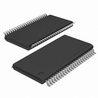
ICS9DB803DGILF IDT, Integrated Device Technology Inc, ICS9DB803DGILF Datasheet - Page 9

ICS9DB803DGILF
Manufacturer Part Number
ICS9DB803DGILF
Description
IC BUFFER 8OUTPUT DIFF 48-TSSOP
Manufacturer
IDT, Integrated Device Technology Inc
Type
Clock Bufferr
Series
-r
Datasheet
1.ICS9DB803DGILFT.pdf
(21 pages)
Specifications of ICS9DB803DGILF
Input
HCSL
Output
HCSL, LVDS
Frequency - Max
400MHz
Voltage - Supply
3.135 V ~ 3.465 V
Operating Temperature
-40°C ~ 85°C
Mounting Type
Surface Mount
Package / Case
48-TSSOP
Frequency-max
400MHz
Number Of Elements
1
Supply Current
200mA
Pll Input Freq (min)
50MHz
Pll Input Freq (max)
110MHz
Operating Supply Voltage (typ)
3.3V
Operating Temp Range
-40C to 85C
Package Type
TSSOP
Output Frequency Range
50 to 100MHz
Operating Supply Voltage (min)
3.135V
Operating Supply Voltage (max)
3.465V
Operating Temperature Classification
Industrial
Pin Count
48
Lead Free Status / RoHS Status
Lead free / RoHS Compliant
Lead Free Status / RoHS Status
Compliant, Lead free / RoHS Compliant
Other names
9DB803DGILF
Available stocks
Company
Part Number
Manufacturer
Quantity
Price
Company:
Part Number:
ICS9DB803DGILF
Manufacturer:
TI
Quantity:
130
Part Number:
ICS9DB803DGILFT
Manufacturer:
IDT
Quantity:
20 000
IDT
Electrical Characteristics - DIF 0.7V Current Mode Differential Pair
1
2
accuracy requirements. The 9DB403/803 itself does not contribute to ppm error.
3
4
5
6
7
T
Guaranteed by design and characterization, not 100% tested in production.
I
All Long Term Accuracy specifications are guaranteed with the assumption that the input clock complies with CK409/CK410/CK505
A
REF
Applies to Bypass Mode Only
Measured from differential waveform
See http://www.pcisig.com for complete specs
Device driven by HP81134A Pulse Generator
ICS9DB803DI
Eight Output Differential Buffer for PCIe for Gen 2
TM
= -40 - 85°C; V
Current Source Output
Crossing Voltage (abs)
Crossing Voltage (var)
/ICS
= V
Jitter, Cycle to cycle
Rise Time Variation
Fall Time Variation
Long Accuracy
PARAMETER
DD
TM
Voltage High
Jitter, Phase
Voltage Low
Max Voltage
Min Voltage
Impedance
Duty Cycle
Rise Time
/(3xR
Fall Time
Eight Output Differential Buffer for PCIe Gen 2
Skew
R
). For R
DD
= 3.3 V +/-5%; C
R
= 475Ω (1%), I
Vcross(abs)
t
SYMBOL
d-Vcross
jphasebypass
t
jphasePLL
VHigh
t
VLow
Vovs
Vuds
ppm
jcyc-cyc
Zo
L
d-t
d-t
t
d
sk3
t
t
=2pF, R
r
f
t3
1
r
f
REF
= 2.32mA. I
S
Statistical measurement on single ended signal
=33.2Ω, R
Measurement on single ended signal using
Measurement from differential wavefrom
Variation of crossing over all edges
using oscilloscope math function.
BYPASS mode as additive jitter
see Tperiod min-max values
V
V
OH
OL
P
OH
=49.9Ω, R
= 6 x I
= 0.175V, V
= 0.525V V
PCIe Gen 1 specs
PCIe Gen 2 specs
PCIe Gen 1 specs
PCIe Gen 2 specs
(pk to pk value)
(pk to pk value)
absolute value.
CONDITIONS
(rms value)
(rms value)
PLL mode
V
REF
V
T
O
= 50%
REF
and V
= V
9
=475Ω
OL
OH
x
= 0.175V
= 0.525V
OH
= 0.7V @ Z
O
=50Ω.
3000
-150
-300
MIN
660
250
175
175
45
TYP
2.6
2.8
ICS9DB803DI
50
40
15
30
40
1150
MAX
850
150
550
140
700
700
125
125
3.1
3.1
60
50
50
86
86
55
0
REV A 06/18/08
UNITS NOTES
ppm
mV
mV
mV
mV
ps
ps
ps
ps
ps
ps
ps
ps
ps
ps
ps
%
Ω
1,6,7
1,6,7
1,6,7
1,6,7
1,3
1,3
1,2
1,5
1,5
1
1
1
1
1
1
1
1
1
1
1


