ICS950602CG IDT, Integrated Device Technology Inc, ICS950602CG Datasheet - Page 9
ICS950602CG
Manufacturer Part Number
ICS950602CG
Description
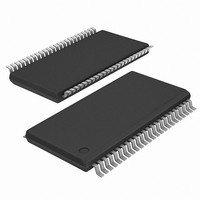
IC TIMING CTRL HUB P4 48-TSSOP
Manufacturer
IDT, Integrated Device Technology Inc
Type
Timing Control Hubr
Datasheet
1.ICS950602CFLFT.pdf
(16 pages)
Specifications of ICS950602CG
Input
Crystal
Output
Clock
Frequency - Max
200MHz
Voltage - Supply
3.135 V ~ 3.465 V
Operating Temperature
0°C ~ 70°C
Mounting Type
Surface Mount
Package / Case
48-TSSOP
Frequency-max
200MHz
Lead Free Status / RoHS Status
Contains lead / RoHS non-compliant
Other names
950602CG


Stresses above those listed under Absolute Maximum Ratings may cause permanent damage to the device. These ratings are
stress specifications only and functional operation of the device at these or any other conditions above those listed in the
operational sections of the specifications is not implied. Exposure to absolute maximum rating conditions for extended
periods may affect product reliability.
Absolute Maximum Ratings
0469B—12/18/02
1
Electrical Characteristics - Input/Supply/Common Output Parameters
T
Powerdown Current
Guaranteed by design, not 100% tested in production.
Input Capacitance
A
Input High Voltage
Input High Current
Input Low Voltage
Input Low Current
Operating Supply
Clk Stabilization
Input Frequency
Transition time
= 0 - 70°C; Supply Voltage V
Pin Inductance
PARAMETER
Supply Voltage . . . . . . . . . . . . . . . . . . . . . . . . . . . 5.5 V
Logic Inputs . . . . . . . . . . . . . . . . . . . . . . . . . . . . . GND –0.5 V to V
Ambient Operating Temperature . . . . . . . . . . . . 0°C to +70°C
Case Temperature . . . . . . . . . . . . . . . . . . . . . . . . 115°C
Storage Temperature . . . . . . . . . . . . . . . . . . . . . –65°C to +150°C
Settling time
Current
Delay
Integrated
Circuit
Systems, Inc.
1
1
1
1
1
SYMBOL
t
t
I
I
PZH
PHZ
DD3.3OP
DD3.3PD
T
C
T
C
L
V
C
V
I
I
STAB
I
trans
T
F
IL1
IL2
OUT
IH
pin
INX
,t
,t
IH
IL
IN
s
i
PZL
PLZ
DD
V
V
V
C
C
IREF = 2.32 mA
IREF = 5 mA
V
Logic Inputs
Output pin capacitance
X1 & X2 pins
To 1st crossing of target frequency
From 1st crossing to 1% target frequency
From V
Output enable delay (all outputs)
Output disable delay (all outputs)
IN
IN
IN
DD
L
L
= 3.3 V +/-5%
= 0 pF; Select @ 67 MHz
=Full load, SDRAM not running
= V
= 0 V; Inputs with no pull-up resistors
= 0 V; Inputs with pull-up resistors
= 3.3 V
DD
DD
= 3.3 V to 1% target frequency
CONDITIONS
9
DD
+0.5 V
V
SS
-200
MIN
27
-5
-5
2
1
1
- 0.3
14.32
TYP
144
22
V
DD
MAX
100
280
0.8
ICS950602
20
37
45
10
10
5
7
5
6
3
3
3
+ 0.3
UNITS
MHz
mA
mA
mA
mA
nH
ms
ms
ms
pF
pF
pF
ns
ns
V
V
Related parts for ICS950602CG
Image
Part Number
Description
Manufacturer
Datasheet
Request
R

Part Number:
Description:
TRANSLATION DEVICE DPI 80-PQFP
Manufacturer:
IDT, Integrated Device Technology Inc
Datasheet:
Part Number:
Description:
IDT PART
Manufacturer:
IDT, Integrated Device Technology Inc
Datasheet:
Part Number:
Description:
IC LIU T1/E1/J1 OCTAL 256PBGA
Manufacturer:
IDT, Integrated Device Technology Inc
Datasheet:

Part Number:
Description:
IC FREQ TIMING GENERATOR 28TSSOP
Manufacturer:
IDT, Integrated Device Technology Inc
Datasheet:
Part Number:
Description:
IC CLK DVR PLL 1:10 40VFQFPN
Manufacturer:
IDT, Integrated Device Technology Inc
Datasheet:
Part Number:
Description:
IC CLK FANOUT BUFFER 1:18 32LQFP
Manufacturer:
IDT, Integrated Device Technology Inc
Datasheet:
Part Number:
Description:
IC CLK FANOUT BUFFER 1:18 32LQFP
Manufacturer:
IDT, Integrated Device Technology Inc
Datasheet:
Part Number:
Description:
IC CK505 VREG/RES 56TSSOP
Manufacturer:
IDT, Integrated Device Technology Inc
Datasheet:

Part Number:
Description:
IC SDRAM CLK DVR 1:10 48-TSSOP
Manufacturer:
IDT, Integrated Device Technology Inc
Datasheet:

Part Number:
Description:
IC CLK DVR PLL 1:10 48TSSOP
Manufacturer:
IDT, Integrated Device Technology Inc
Datasheet:
Part Number:
Description:
IC FLEXPC CLK PROGR P4 56-TSSOP
Manufacturer:
IDT, Integrated Device Technology Inc
Datasheet:
Part Number:
Description:
IC FLEXPC CLK PROGR P4 56-TSSOP
Manufacturer:
IDT, Integrated Device Technology Inc
Datasheet:
Part Number:
Description:
IC FLEXPC CLK PROGR P4 56-SSOP
Manufacturer:
IDT, Integrated Device Technology Inc
Datasheet:

Part Number:
Description:
IC PLL CLK DRIVER 2.5V 28-TSSOP
Manufacturer:
IDT, Integrated Device Technology Inc
Datasheet:
Part Number:
Description:
IC CLOCK DRIVER 2.5V 24-TSSOP
Manufacturer:
IDT, Integrated Device Technology Inc
Datasheet: