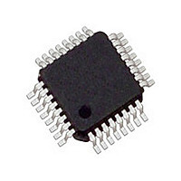
MPC940LACR2 IDT, Integrated Device Technology Inc, MPC940LACR2 Datasheet - Page 6

MPC940LACR2
Manufacturer Part Number
MPC940LACR2
Description
IC CLK FANOUT BUFFER 1:18 32LQFP
Manufacturer
IDT, Integrated Device Technology Inc
Type
Clock Distributionr
Datasheet
1.MPC940LAC.pdf
(11 pages)
Specifications of MPC940LACR2
Input
LVCMOS, LVPECL
Output
LVCMOS
Frequency - Max
250MHz
Voltage - Supply
2.375 V ~ 3.465 V
Operating Temperature
0°C ~ 70°C
Mounting Type
Surface Mount
Package / Case
32-LQFP
Frequency-max
250MHz
Number Of Clock Inputs
2
Output Frequency
250MHz
Output Logic Level
LVCMOS
Operating Supply Voltage (min)
2.375V
Operating Supply Voltage (typ)
2.5/3.3V
Operating Supply Voltage (max)
3.465V
Package Type
TQFP
Operating Temp Range
0C to 70C
Operating Temperature Classification
Commercial
Signal Type
LVCMOS/LVPECL
Mounting
Surface Mount
Pin Count
32
Quiescent Current
1mA
Lead Free Status / RoHS Status
Lead free / RoHS Compliant
Available stocks
Company
Part Number
Manufacturer
Quantity
Price
Company:
Part Number:
MPC940LACR2
Manufacturer:
IDT, Integrated Device Technology Inc
Quantity:
10 000
IDT™ / ICS™ 1:18 CLOCK DISTRIBUTION CHIP
MPC940L
LOW VOLTAGE 1:18 CLOCK DISTRIBUTION CHIP
PCLK_CLK
PCLK_CLK
Figure 3. Propagation Delay (t
Figure 7. Output Transition Time Test Reference
The time from the PLL controlled edge to the non controlled
edge, divided by the time between PLL controlled edges,
expressed as a percentage.
t
F
Q
Figure 5. Output Duty Cycle (DC)
Figure 1. LVCMOS_CLK MPC940L AC Test Reference for V
Figure 2. PECL_CLK MPC940L AC Test Reference for V
t
P
V
PP
t
PD
Generator
Z = 50Ω
T
Differential Pulse
0
Pulse
DC = t
Generator
Z = 50Ω
t
R
P
/T
PD
V
0
CC
) Test Reference
x 100%
0.55
2.4
= 3.3 V V
Z
O
= 50Ω
CC
Z
1.8 V
0.6 V
V
V
GND
= 2.5 V
O
R
V
CC
CC
T
= 50Ω
TT
V
V
GND
V
= 50Ω
÷ 2
CC
CC
CMR
R
T
÷2
= 50Ω
V
TT
MPC940L DUT
6
LVCMOS_CLK
MPC940L DUT
The pin-to-pin skew is defined as the worst case difference
in propagation delay between any two similar delay paths
within a single device.
Figure 8. Input Transition Time Test Reference
t
F
Figure 4. LVCMOS Propagation Delay (t
Figure 6. Output-to-Output Skew T
Q
CC
CC
= 3.3 V and V
Z
= 3.3 V and V
O
= 50Ω
Test Reference
Z
O
t
PD
= 50Ω
R
T
= 50Ω
CC
R
t
CC
T
SK(O)
t
R
= 50Ω
= 2.5 V
V
= 2.5 V
V
TT
CC
MPC940L REV 7 JUNE 5, 2007
2.0
0.8
= 3.3 V V
V
TT
SK(O)
CC
1.7 V
0.7 V
= 2.5 V
PD
V
V
GND
V
V
GND
CC
CC
OH
CC
)
V
V
GND
V
V
GND
CC
CC
CC
CC
÷ 2
÷ 2
÷ 2
÷ 2


