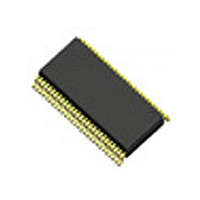
IDTCV125PAG IDT, Integrated Device Technology Inc, IDTCV125PAG Datasheet - Page 3

IDTCV125PAG
Manufacturer Part Number
IDTCV125PAG
Description
IC FLEXPC CLK PROGR P4 56-TSSOP
Manufacturer
IDT, Integrated Device Technology Inc
Type
PC Clockr
Series
FlexPC™r
Datasheet
1.IDTCV125PAG8.pdf
(24 pages)
Specifications of IDTCV125PAG
Input
Crystal
Output
Clock
Frequency - Max
400MHz
Voltage - Supply
3.135 V ~ 3.465 V
Operating Temperature
0°C ~ 70°C
Mounting Type
Surface Mount
Package / Case
56-TSSOP
Frequency-max
400MHz
Number Of Elements
4
Supply Current
400mA
Pll Input Freq (min)
14.31818MHz
Operating Supply Voltage (typ)
3.3V
Operating Temp Range
0C to 70C
Package Type
TSSOP
Output Frequency Range
100 to 400MHz
Operating Supply Voltage (min)
3.135V
Operating Supply Voltage (max)
3.465V
Operating Temperature Classification
Commercial
Pin Count
56
Lead Free Status / RoHS Status
Lead free / RoHS Compliant
Other names
CV125PAG
PIN DESCRIPTION
IDTCV125
PROGRAMMABLE FLEXPC CLOCK FOR P4 PROCESSOR
Pin Number
10
11
12
13
14
15
16
17
18
19
20
21
22
23
24
25
26
27
28
29
30
31
32
33
34
35
36
37
38
39
40
41
42
1
2
3
4
5
6
7
8
9
CPU2_ITP#/SRC7#
PCIF1/SEL100/96#
FSB/TEST_MODE
CPU2_ITP/SRC7
V
PCIF0/ITP_EN
TT
USB48/FSA
V
V
V
V
V
V
V
_P
V
V
DOT96#
CPU1#
LVDS#
SRC1#
SRC2#
SRC3#
SRC4#
SRC5#
SRC6#
DD
DD
DD
DD
DOT96
SS
V
SRC1
SRC2
SRC3
SRC4
SRC5
SRC6
CPU1
Name
DD
DD
LVDS
SS
SS
V
PCI1
PCI2
PCI3
V
V
WRGD
I
DD
SS
_SRC
REF
_SRC
_SRC
_SRC
_CPU
DDA
_PCI
_PCI
SSA
_PCI
_PCI
48
48
#/PD
Type
PWR
GND
GND
PWR
PWR
GND
PWR
PWR
GND
PWR
PWR
GND
PWR
OUT
OUT
OUT
OUT
OUT
OUT
OUT
OUT
OUT
OUT
OUT
OUT
OUT
OUT
OUT
OUT
OUT
OUT
OUT
OUT
OUT
OUT
OUT
OUT
I/O
I/O
I/O
I N
I N
3.3V
GND
PCI clock
PCI clock
PCI clock
GND
3.3V
PCI clock, free running. CPU2 select (sampled on V
PCI clock, free running. SEL100/96MHz (sampled on V
Level-sensitive strobe used to latch the FSA, FSB, FSC/TEST_SEL, and PCIF0/ITP_EN inputs. After
V
SEL100/96# input.
3.3V
48MHz clock/FSA for CPU frequency selection
GND
96MHz 0.7 current mode differential clock output
96MHz 0.7 current mode differential clock output
CPU frequency selection. Selects R
Differential serial reference clock
Differential serial reference clock
Differential serial reference clock
Differential serial reference clock
3.3V
Differential serial reference clock
Differential serial reference clock
Differential serial reference clock
Differential serial reference clock
Differential serial reference clock
Differential serial reference clock
3.3V
GND
Differential serial reference clock
Differential serial reference clock
Differential serial reference clock
Differential serial reference clock
3.3V
Selectable CPU or SRC differential clock output. ITP_EN = 0 at V
Selectable CPU or SRC differential clock output. ITP_EN = 0 at V
3.3V
GND
Reference current for differential output buffer
Host 0.7 current mode differential clock output
Host 0.7 current mode differential clock output
3.3V
TT
_P
WRGD
# assertion, becomes a real-time input for asserting power down. (Active HIGH). Latch PCIF1/
3
EF
/N or Hi-Z when in test mode, Hi-Z = 1, R
Description
COMMERCIAL TEMPERATURE RANGE
TT
TT
_P
_P
WRGD
WRGD
# assertion) HIGH = CPU2.
# assertion) HIGH, LVDS = 100MHz.
TT
TT
_P
_P
WRGD
WRGD
# assertion = SRC7#.
# assertion = SRC7.
EF
/N = 0.


