AD9548BCPZ Analog Devices Inc, AD9548BCPZ Datasheet - Page 54
AD9548BCPZ
Manufacturer Part Number
AD9548BCPZ
Description
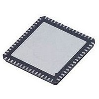
IC CLOCK GEN/SYNCHRONIZR 88LFCSP
Manufacturer
Analog Devices Inc
Datasheet
1.AD9548BCPZ-REEL7.pdf
(112 pages)
Specifications of AD9548BCPZ
Input
*
Output
*
Frequency - Max
*
Voltage - Supply
*
Operating Temperature
*
Mounting Type
Surface Mount
Package / Case
88-LFCSP
Frequency-max
*
Clock Ic Type
Clock Synthesizer
Ic Interface Type
Serial
Frequency
1GHz
No. Of Outputs
4
No. Of Multipliers / Dividers
4
Supply Current
190mA
Lead Free Status / RoHS Status
Lead free / RoHS Compliant
Available stocks
Company
Part Number
Manufacturer
Quantity
Price

Part Number:
AD9548BCPZ
Manufacturer:
ADI/亚德诺
Quantity:
20 000
Company:
Part Number:
AD9548BCPZ-SMD7
Manufacturer:
SHARP
Quantity:
392


AD9548
SCLK
Table 32. Serial Control Port Timing
Parameter
t
t
t
t
t
t
t
t
SDIO
DS
DH
CLK
S
C
HI
LO
DV
CS
DON'T CARE
DON'T CARE
A0 A1 A2 A3
SCLK
SDIO
CS
Description
Setup time between data and the rising edge of SCLK
Hold time between data and the rising edge of SCLK
Period of the clock
Setup time between the CS falling edge and the SCLK rising edge (start of the communication cycle)
Setup time between the SCLK rising edge and CS rising edge (end of the communication cycle)
Minimum period that SCLK should be in a logic high state
Minimum period that SCLK should be in a logic low state
SCLK to valid SDIO and SDO (see Figure 56)
A4
16-BIT INSTRUCTION HEADER
A5 A6 A7 A8
t
Figure 57. Serial Control Port Write—LSB First, 16-Bit Instruction, Two Bytes of Data
t
DS
S
SCLK
SDIO
SDO
CS
BIT N
Figure 56. Timing Diagram for Serial Control Port Register Read
A9 A10 A11 A12
t
HI
t
DH
Figure 58. Serial Control Port Timing—Write
DATA BIT N
t
CLK
W0
t
Rev. A | Page 54 of 112
DV
t
LO
W1
R/W
BIT N + 1
D0
DATA BIT N – 1
D1
REGISTER (N) DATA
D2 D3 D4
D5 D6 D7
D0
D1 D2
REGISTER (N + 1) DATA
D3 D4 D5
t
C
D6
D7
DON'T CARE
DON'T CARE
Related parts for AD9548BCPZ
Image
Part Number
Description
Manufacturer
Datasheet
Request
R

Part Number:
Description:
Clock Generator Evaluation Board
Manufacturer:
Analog Devices Inc
Datasheet:


Part Number:
Description:
±1.7g Dual-Axis IMEMS Accelerometer Evaluation Board
Manufacturer:
Analog Devices Inc
Datasheet:
Part Number:
Description:
Inertial Sensor Evaluation System
Manufacturer:
Analog Devices Inc
Datasheet:
Part Number:
Description:
Manufacturer:
Analog Devices Inc
Datasheet:
Part Number:
Description:
Manufacturer:
Analog Devices Inc
Datasheet:
Part Number:
Description:
Manufacturer:
Analog Devices Inc
Datasheet:
Part Number:
Description:
Manufacturer:
Analog Devices Inc
Datasheet:
Part Number:
Description:
Manufacturer:
Analog Devices Inc
Datasheet:
Part Number:
Description:
Manufacturer:
Analog Devices Inc
Datasheet:
Part Number:
Description:
Manufacturer:
Analog Devices Inc
Datasheet:
Part Number:
Description:
Manufacturer:
Analog Devices Inc
Datasheet:
Part Number:
Description:
Manufacturer:
Analog Devices Inc
Datasheet: