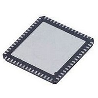
AD9548BCPZ Analog Devices Inc, AD9548BCPZ Datasheet - Page 52

AD9548BCPZ
Manufacturer Part Number
AD9548BCPZ
Description
IC CLOCK GEN/SYNCHRONIZR 88LFCSP
Manufacturer
Analog Devices Inc
Datasheet
1.AD9548BCPZ-REEL7.pdf
(112 pages)
Specifications of AD9548BCPZ
Input
*
Output
*
Frequency - Max
*
Voltage - Supply
*
Operating Temperature
*
Mounting Type
Surface Mount
Package / Case
88-LFCSP
Frequency-max
*
Clock Ic Type
Clock Synthesizer
Ic Interface Type
Serial
Frequency
1GHz
No. Of Outputs
4
No. Of Multipliers / Dividers
4
Supply Current
190mA
Lead Free Status / RoHS Status
Lead free / RoHS Compliant
Available stocks
Company
Part Number
Manufacturer
Quantity
Price
Part Number:
AD9548BCPZ
Manufacturer:
ADI/亚德诺
Quantity:
20 000
Company:
Part Number:
AD9548BCPZ-SMD7
Manufacturer:
SHARP
Quantity:
392
AD9548
SPI Mode Operation
The SPI port supports both 3-wire (bidirectional) and 4-wire
(unidirectional) hardware configurations and both MSB-first
and LSB-first data formats. Both the hardware configuration
and data format features are programmable. By default, the
AD9548 uses the bidirectional MSB-first mode. The reason that
bidirectional is the default mode is so that the user can still
write to the device, if it is wired for unidirectional operation, to
switch to unidirectional mode.
Assertion (active low) of the CS pin initiates a write or read
operation to the AD9548 SPI port. For data transfers of three
bytes or fewer (excluding the instruction word), the device
supports the CS stalled high mode (see
the
allowing time for the system controller to process the next byte.
CS can be deasserted only on byte boundaries, however. This
applies to both the instruction and data portions of the transfer.
During stall high periods, the serial control port state machine
enters a wait state until all data is sent. If the system controller
decides to abort a transfer midstream, then the state machine must
be reset by either completing the transfer or by asserting the CS
pin for at least one complete SCLK cycle (but less than eight
SCLK cycles). Deasserting the CS pin on a nonbyte boundary
terminates the serial transfer and flushes the buffer.
In the streaming mode (see Table 29), any number of data bytes
can be transferred in a continuous stream. The register address
is automatically incremented or decremented. CS must be
deasserted at the end of the last byte transferred, thereby ending
the stream mode.
Table 29. Byte Transfer Count
W1
0
0
1
1
Communication Cycle—Instruction Plus Data
The SPI protocol consists of a two-part communication cycle.
The first part is a 16-bit instruction word that is coincident with
the first 16 SCLK rising edges and a payload. The instruction
word provides the AD9548 serial control port with information
regarding the payload. The instruction word includes the R/ W
bit that indicates the direction of the payload transfer (that is, a
read or write operation). The instruction word also indicates
the number of bytes in the payload and the starting register
address of the first payload byte.
CS pin can be temporarily deasserted on any byte boundary,
W0
0
1
0
1
Bytes to Transfer
1
2
3
Streaming mode
Table 29
). In this mode,
Rev. A | Page 52 of 112
Write
If the instruction word indicates a write operation, the payload
is written into the serial control port buffer of the AD9548. Data
bits are registered on the rising edge of SCLK. The length of the
transfer (1, 2, or 3 bytes or streaming mode) depends on the W0
and W1 bits (see Table 29) in the instruction byte. When not
streaming, CS can be deasserted after each sequence of eight
bits to stall the bus (except after the last byte, where it ends the
cycle). When the bus is stalled, the serial transfer resumes when
CS is asserted. Deasserting the CS pin on a nonbyte boundary
resets the serial control port. Reserved or blank registers are not
skipped over automatically during a write sequence. Therefore,
the user must know what bit pattern to write to the reserved
registers to preserve proper operation of the part. Generally, it
does not matter what data is written to blank registers, but it is
customary to write 0s.
Most of the serial port registers are buffered (see the
Buffered/Active Registers section for details on the difference
between buffered and active registers). Therefore, data written
into buffered registers does not take effect immediately. An
additional operation is needed to transfer buffered serial control
port contents to the registers that actually control the device.
This is accomplished with an I/O update operation, which is
performed in one of two ways. One is by writing a Logic 1 to
Register 0005, Bit 0 (this bit is self-clearing). The other is to use
an external signal via an appropriately programmed
multifunction pin. The user can change as many register bits as
desired before executing an I/O update. The I/O update operation
transfers the buffer register contents to their active register
counterparts.
Read
The AD9548 supports the long instruction mode only. If the
instruction word indicates a read operation, the next N × 8
SCLK cycles clock out the data from the address specified in the
instruction word. N is the number of data bytes read and
depends on the W0 and W1 bits of the instruction word. The
readback data is valid on the falling edge of SCLK. Blank
registers are not skipped over during readback.
A readback operation takes data from either the serial control
port buffer registers or the active registers, as determined by
Register 0004, Bit 0.
SPI Instruction Word (16 Bits)
The MSB of the 16-bit instruction word is R/
whether the instruction is a read or a write. The next two bits,
W1 and W0, indicate the number of bytes in the transfer (see
Table 29
which indicates the starting register address of the read/write
operation (see
). The final 13 bits are the register address (A12 to A0),
Table 31
).
W
, which indicates


