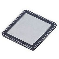
AD9548BCPZ Analog Devices Inc, AD9548BCPZ Datasheet - Page 102

AD9548BCPZ
Manufacturer Part Number
AD9548BCPZ
Description
IC CLOCK GEN/SYNCHRONIZR 88LFCSP
Manufacturer
Analog Devices Inc
Datasheet
1.AD9548BCPZ-REEL7.pdf
(112 pages)
Specifications of AD9548BCPZ
Input
*
Output
*
Frequency - Max
*
Voltage - Supply
*
Operating Temperature
*
Mounting Type
Surface Mount
Package / Case
88-LFCSP
Frequency-max
*
Clock Ic Type
Clock Synthesizer
Ic Interface Type
Serial
Frequency
1GHz
No. Of Outputs
4
No. Of Multipliers / Dividers
4
Supply Current
190mA
Lead Free Status / RoHS Status
Lead free / RoHS Compliant
Available stocks
Company
Part Number
Manufacturer
Quantity
Price
Part Number:
AD9548BCPZ
Manufacturer:
ADI/亚德诺
Quantity:
20 000
Company:
Part Number:
AD9548BCPZ-SMD7
Manufacturer:
SHARP
Quantity:
392
AD9548
Table 145. EEPROM Storage Sequence for Clock Distribution Settings
Address
0E1B
0E1C
0E1D
0E1E
Table 146. EEPROM Storage Sequence for Reference Input Settings
Address
0E1F
0E20
0E21
Table 147. EEPROM Storage Sequence for Profile 0 and Profile 1 Settings
Address
0E22
0E23
0E24
Bits
[7:0]
[7:0]
[7:0]
[7:0]
Bits
[7:0]
[7:0]
[7:0]
Bits
[7:0]
[7:0]
[7:0]
Clock distribution
Clock distribution
I/O update
Reference inputs
Reference inputs
Profile 0 and Profile 1
Profile 0 and Profile 1
Bit Name
Bit Name
Bit Name
Description
The default value of this register is 0x19, which the controller interprets as a data
instruction. Its decimal value is 25, which tells the controller to transfer 26 bytes of
data (25 + 1) beginning at the address specified by the next two bytes. The
controller stores 0x19 in the EEPROM and increments the EEPROM address pointer.
The default value of these two registers is 0x0400. Note that Register 0E1C and
Register 0E1D are the most significant and least significant bytes of the target
address, respectively. Because the previous register contains a data instruction,
these two registers define a starting address (in this case, 0x0400). The controller
stores 0x0400 in the EEPROM and increments the EEPROM pointer by 2. It then
transfers
26 bytes from the register map (beginning at Address 0x0400) to the EEPROM and
increments the EEPROM address pointer by 27 (26 data bytes and one checksum
byte). The 26 bytes transferred correspond to the clock distribution parameters in
the register map.
The default value of this register is 0x80, which the controller interprets as an I/O
update instruction. The controller stores 0x80 in the EEPROM and increments the
EEPROM address pointer.
Description
The default value of this register is 0x07, which the controller interprets as a data
instruction. Its decimal value is 7, which tells the controller to transfer eight bytes
of data (7 + 1) beginning at the address specified by the next two bytes. The
controller stores 0x07 in the EEPROM and increments the EEPROM address pointer.
The default value of these two registers is 0x0500. Note that Register 0E20 and
Register 0E21 are the most significant and least significant bytes of the target
address, respectively. Because the previous register contains a data instruction,
these two registers define a starting address (in this case, 0x0500). The controller
stores 0x0500 in the EEPROM and increments the EEPROM pointer by 2. It then
transfers eight bytes from the register map (beginning at Address 0x0500) to the
EEPROM and increments the EEPROM address pointer by nine (eight data bytes
and one checksum byte). The eight bytes transferred correspond to the reference
inputs parameters in the register map.
Description
The default value of this register is 0x63, which the controller interprets as a data
instruction. Its decimal value is 99, which this tells the controller to transfer 100
bytes of data (99 + 1) beginning at the address specified by the next two bytes. The
controller stores 0x63 in the EEPROM and increments the EEPROM address pointer.
The default value of these two registers is 0x0600. Note that Register 0E23 and
Register 0E24 are the most significant and least significant bytes of the target
address, respectively. Because the previous register contains a data instruction,
these two registers define a starting address (in this case, 0x0600). The controller
stores 0x0600 in the EEPROM and increments the EEPROM pointer by 2. It then
transfers 100 bytes from the register map (beginning at Address 0x0600) to the
EEPROM and increments the EEPROM address pointer by 101 (100 data bytes and
Profile 1 parameters in the register map.
one checksum byte). The 99 bytes transferred correspond to the Profile 0 and
Rev. A | Page 102 of 112


