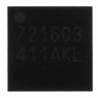
ICS9DBL411AKLFT IDT, Integrated Device Technology Inc, ICS9DBL411AKLFT Datasheet - Page 6

ICS9DBL411AKLFT
Manufacturer Part Number
ICS9DBL411AKLFT
Description
IC FANOUT BUFFER 4OUTPUT 20-MLF
Manufacturer
IDT, Integrated Device Technology Inc
Type
Fanout Bufferr
Datasheet
1.ICS9DBL411AKLFT.pdf
(9 pages)
Specifications of ICS9DBL411AKLFT
Input
Differential
Output
Differential
Frequency - Max
400MHz
Voltage - Supply
3.135 V ~ 3.465 V
Operating Temperature
0°C ~ 70°C
Mounting Type
Surface Mount
Package / Case
20-MLF®, QFN
Frequency-max
400MHz
Number Of Elements
1
Supply Current
54mA
Pll Input Freq (min)
33MHz
Pll Input Freq (max)
400MHz
Operating Supply Voltage (typ)
3.3V
Operating Temp Range
0C to 70C
Package Type
VFQFPN EP
Operating Supply Voltage (min)
3.135V
Operating Supply Voltage (max)
3.465V
Operating Temperature Classification
Commercial
Pin Count
20
Lead Free Status / RoHS Status
Lead free / RoHS Compliant
Other names
800-1824-2
9DBL411AKLFT
9DBL411AKLFT
Available stocks
Company
Part Number
Manufacturer
Quantity
Price
Company:
Part Number:
ICS9DBL411AKLFT
Manufacturer:
VISHAY
Quantity:
17 087
IDT
1
2
3
4
5
falling edge of CLK#. It is measured using a +/-75mV window centered on the average cross point where CLK meets CLK#.
6
7
8
Notes on Electrical Characteristics:
AC Electrical Characteristics - DIF Low Power Differential Outputs
Guaranteed by design and characterization, not 100% tested in production.
Slew rate measured through Vswing centered around differential zero
Vxabs is defined as the voltage where CLK = CLK#
Only applies to the differential rising edge (CLK rising and CLK# falling)
Defined as the total variation of all crossing voltages of CLK rising and CLK# falling. Matching applies to rising edge rate of CLK and
Tthis is the figure refers to the maximum distortion of the input wave form.
Operation under these conditions is neither implied, nor guaranteed.
Maximum input voltage is not to exceed maximum VDD
ICS9DBL411A
Four Output Differential Buffer for PCI Express
DIF Jitter - Cycle to Cycle
TM
Maximum Output Voltage
Differential Voltage Swing
PCIe Gen2 Phase Jitter -
PCIe Gen2 Phase Jitter -
Minimum Output Voltage
Crossing Point Variation
Falling Edge Slew Rate
Rising Edge Slew Rate
Crossing Point Voltage
Duty Cycle Distortion
Slew Rate Variation
Propagation Delay
Four Output Differential Buffer for PCI Express
DIF[3:0] Skew
PARAMETER
Addtive
Addtive
t
t
SYMBOL
V
phase_addLO
DIF
phase_addHI
D
D
D
DIFJ
V
XABSVAR
t
V
V
V
CYCDIS0
CYCDIS1
CYCDIS2
SLVAR
t
t
SWING
XABS
t
SLR
FLR
HIGH
LOW
PD
SKEW
C2C
1.5MHz < fIN < Nyquist (50MHz)
Single-ended Measurement
Single-ended Measurement
Single-ended Measurement
Differential Measurement,
Differential Measurement,
Differential Measurement,
Differential Measurement
Differential Measurement
Differential Measurement
Differential Measurement
Differential Measurement
100MHz < fIN<=267MHz
10KHz < fIN < 1.5MHz
Includes undershoot
Input to output Delay
Includes overshoot
CONDITIONS
fIN<=100MHz
fIN>267MHz
Additive
6
1200
-300
MIN
300
2.5
1
1
1150
MAX
550
140
2.5
2.5
0.5
3.5
0.8
0.1
20
+5
+7
25
50
Advance Information
ps rms
ps rms
UNITS
V/ns
V/ns
mV
mV
mV
mV
mV
ps
ps
ns
%
%
%
%
NOTES
1,3,4
1,3,5
1,2
1,2
1,6
1,6
1,6
1
1
1
1
1
1
1
1
1
1250B—02/21/08


