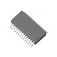
ICS9DB401CGLF IDT, Integrated Device Technology Inc, ICS9DB401CGLF Datasheet - Page 6

ICS9DB401CGLF
Manufacturer Part Number
ICS9DB401CGLF
Description
IC BUFFER 4OUTPUT DIFF 28-TSSOP
Manufacturer
IDT, Integrated Device Technology Inc
Type
Clock Buffer/Driverr
Datasheet
1.ICS9DB401CGLF.pdf
(17 pages)
Specifications of ICS9DB401CGLF
Input
Clock
Output
Clock
Frequency - Max
400MHz
Voltage - Supply
3.135 V ~ 3.465 V
Operating Temperature
0°C ~ 70°C
Mounting Type
Surface Mount
Package / Case
28-TSSOP
Frequency-max
400MHz
Number Of Elements
1
Supply Current
200mA
Pll Input Freq (min)
50MHz
Pll Input Freq (max)
200MHz
Operating Supply Voltage (typ)
3.3V
Operating Temp Range
0C to 70C
Package Type
TSSOP
Output Frequency Range
50 to 200MHz
Operating Supply Voltage (min)
3.135V
Operating Supply Voltage (max)
3.465V
Operating Temperature Classification
Commercial
Pin Count
28
Lead Free Status / RoHS Status
Lead free / RoHS Compliant
Other names
800-1976-5
9DB401CGLF
ICS9DB401CGLF
9DB401CGLF
ICS9DB401CGLF
Available stocks
Company
Part Number
Manufacturer
Quantity
Price
Company:
Part Number:
ICS9DB401CGLFT
Manufacturer:
IDT
Quantity:
3 200
Electrical Characteristics - DIF 0.7V Current Mode Differential Pair
IDT
1
2
complies with CK409/CK410 accuracy requirements
3
T
1
2
T
Electrical Characteristics - Clock Input Parameters
Differential Input High Voltage
Differential Input Low Voltage
Guaranteed by design and characterization, not 100% tested in production.
I
Slew rate measured through Vswing centered around differential zero
All Long Term Accuracy and Clock Period specifications are guaranteed with the assumption that the input clock
A
REF
A
Guaranteed by design and characterization, not 100% tested in production.
Input SRC Jitter - Cycle to
ICS9DB401C
Four Output Differential Buffer for PCI Express
Input Slew Rate - DIF_IN
TM
= 0 - 70°C; V
Crossing Voltage (abs)
= 0 - 70°C; Supply Voltage V
Input Leakage Current
Current Source Output
Crossing Voltage (var)
/ICS
Input Duty Cycle
Jitter, Cycle to cycle
Rise Time Variation
= V
Fall Time Variation
PARAMETER
Long Accuracy
PARAMETER
TM
Voltage High
Voltage Low
Max Voltage
DD
Min Voltage
Impedance
Duty Cycle
Rise Time
Fall Time
Four Output Differential Buffer for PCI Express
Cycle
/(3xR
Skew
DD
R
). For R
= 3.3 V +/-5%; C
R
= 475Ω (1%), I
SYMBOL
SRCJ
Vcross(abs)
V
V
dv/dt
d
IHDIF
ILDIF
I
SYMBOL
d-Vcross
IN
tin
DD
VHigh
C2CIn
VLow
t
Vuds
Vovs
jcyc-cyc
ppm
L
Zo
d-t
d-t
t
d
= 3.3 V +/-5%
sk3
t
t
=2pF, R
r
t3
f
1
r
f
Measurement from differential
REF
(single-ended measurement)
(single-ended measurement)
S
Statistical measurement on single
= 2.32mA. I
=33.2Ω, R
Differential Measurement
ended signal using oscilloscope
BYPASS mode as additive jitter
Measured differentially
Measurement on single ended
Measurement from differential
Measurement from differential
V
Variation of crossing over all
see Tperiod min-max values
V
signal using absolute value.
V
IN
CONDITIONS
Differential inputs
Differential inputs
OL
OH
= V
wavefrom
= 0.175V, V
= 0.525V V
DD ,
CONDITIONS
math function.
P
V
PLL mode,
=49.9Ω, Ι
OH
V
wavefrom
wavefrom
IN
V
T
edges
= GND
= 6 x I
O
= 50%
= V
6
OL
OH
x
REF
REF
= 0.175V
= 0.525V
and V
= 475Ω
V
OH
SS
MIN
600
0.4
45
-5
= 0.7V @ Z
- 300
3000
-150
-300
MIN
660
250
175
175
45
MAX
1150
300
125
55
8
5
O
=50Ω.
TYP
ICS9DB401C
UNITS
V/ns
mV
mV
1150
uA
MAX
%
ps
850
150
550
140
700
700
125
125
50
55
50
50
0
NOTES
UNITS
ppm
1
mV
mV
mV
mV
1
1
2
1
1
ps
ps
ps
ps
ps
ps
ps
%
Ω
REV E 03/18/08
NOTES
1,3
1,3
1,2
1
1
1
1
1
1
1
1
1
1
1
1
1


