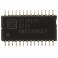
ICS9DB106BGLFT IDT, Integrated Device Technology Inc, ICS9DB106BGLFT Datasheet - Page 3

ICS9DB106BGLFT
Manufacturer Part Number
ICS9DB106BGLFT
Description
IC BUFFER ZD 6OUTPUT 28-TSSOP
Manufacturer
IDT, Integrated Device Technology Inc
Type
Zero Delay Bufferr
Datasheet
1.ICS9DB106BFLFT.pdf
(14 pages)
Specifications of ICS9DB106BGLFT
Input
Clock
Output
HCSL
Frequency - Max
101MHz
Voltage - Supply
3.135 V ~ 3.465 V
Operating Temperature
0°C ~ 70°C
Mounting Type
Surface Mount
Package / Case
28-TSSOP
Frequency-max
101MHz
Lead Free Status / RoHS Status
Lead free / RoHS Compliant
Other names
800-1242-2
9DB106BGLFT
9DB106BGLFT
Pin Description
IDT
Note:
Pins preceeded by '**' have internal 120K ohm pull down resistors
9DB106
Six Output Differential Buffer for PCIe Gen 2
®
PIN #
Six Output Differential Buffer for PCIe Gen 2
10
11
12
13
14
15
16
17
18
19
20
21
22
23
24
25
26
27
28
1
2
3
4
5
6
7
8
9
PLL_BW
CLK_INT
CLK_INC
**CLKREQ1#
PCIEXT0
PCIEXC0
VDD
GND
PCIEXT1
PCIEXC1
PCIEXT2
PCIEXC2
VDD
SMBDAT
SMBCLK
VDD
PCIEXC3
PCIEXT3
PCIEXC4
PCIEXT4
GND
VDD
PCIEXC5
PCIEXT5
**CLKREQ4#
IREF
GNDA
VDDA
PIN NAME
PIN TYPE
PWR
PWR
PWR
PWR
PWR
PWR
PWR
OUT
OUT
OUT
OUT
OUT
OUT
OUT
OUT
OUT
OUT
OUT
OUT
OUT
I/O
IN
IN
IN
IN
IN
IN
IN
3.3V input for selecting PLL Band Width
0 = low, 1= high
True Input for differential reference clock.
Complementary Input for differential reference clock.
Output enable for PCI Express (SRC) outputs. SMBus selects
which outputs are controlled.
0 = enabled, 1 =disabled
True clock of differential PCI_Express pair.
Complementary clock of differential PCI_Express pair.
Power supply, nominal 3.3V
Ground pin.
True clock of differential PCI_Express pair.
Complementary clock of differential PCI_Express pair.
True clock of differential PCI_Express pair.
Complementary clock of differential PCI_Express pair.
Power supply, nominal 3.3V
Data pin of SMBUS circuitry, 5V tolerant
Clock pin of SMBUS circuitry, 5V tolerant
Power supply, nominal 3.3V
Complementary clock of differential PCI_Express pair.
True clock of differential PCI_Express pair.
Complementary clock of differential PCI_Express pair.
True clock of differential PCI_Express pair.
Ground pin.
Power supply, nominal 3.3V
Complementary clock of differential PCI_Express pair.
True clock of differential PCI_Express pair.
Output enable for PCI Express (SRC) outputs. SMBus selects
which outputs are controlled.
0 = enabled, 1 =disabled
This pin establishes the reference for the differential current-mode
output pairs. It requires a fixed precision resistor to ground.
475ohm is the standard value for 100ohm differential impedance.
Other impedances require different values. See data sheet.
Ground pin for the PLL core.
3.3V power for the PLL core.
3
DESCRIPTION
9DB106
REV J 01/27/11


