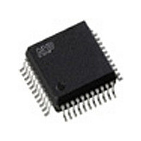
SAA7113HV2 NXP Semiconductors, SAA7113HV2 Datasheet - Page 21

SAA7113HV2
Manufacturer Part Number
SAA7113HV2
Description
Manufacturer
NXP Semiconductors
Datasheet
1.SAA7113HV2.pdf
(75 pages)
Specifications of SAA7113HV2
Video Resolution (max)
720Pixels
Pin Count
44
Package Type
PQFP
Lead Free Status / RoHS Status
Compliant
- Current page: 21 of 75
- Download datasheet (367Kb)
Philips Semiconductors
9397 750 14232
Product data sheet
8.6 Clock generation circuit
The internal CGC generates all clock signals required for the video input processor. The
internal signal LFCO is a digital-to-analog converted signal provided by the horizontal
PLL. It is the multiple of the line frequency: 6.75 MHz = 429
6.75 MHz = 432
Internally the LFCO signal is multiplied by a factor of 2 and 4 in the PLL circuit (including
phase detector, loop filtering, VCO and frequency divider) to obtain the output clock
signals. The rectangular output clocks have a 50 % duty factor.
Table 4:
Clock
XTAL
LLC
LLC2 (internal)
LLC4 (internal)
LLC8 (virtual)
Fig 20. Block diagram of clock generation circuit
LFCO
Clock frequencies
BAND PASS
FC = LLC/4
f
H
(60 Hz).
Rev. 02 — 9 May 2005
DETECTION
CROSS
ZERO
DETECTION
PHASE
Frequency (MHz)
24.576
27
13.5
6.75
3.375
DIVIDER
FILTER
LOOP
© Koninklijke Philips Electronics N.V. 2005. All rights reserved.
1/2
9-bit video input processor
f
H
(50 Hz) or
SAA7113H
OSCILLATOR
DIVIDER
1/2
mhb330
21 of 75
LLC
LLC2
Related parts for SAA7113HV2
Image
Part Number
Description
Manufacturer
Datasheet
Request
R
Part Number:
Description:
NXP Semiconductors designed the LPC2420/2460 microcontroller around a 16-bit/32-bitARM7TDMI-S CPU core with real-time debug interfaces that include both JTAG andembedded trace
Manufacturer:
NXP Semiconductors
Datasheet:

Part Number:
Description:
NXP Semiconductors designed the LPC2458 microcontroller around a 16-bit/32-bitARM7TDMI-S CPU core with real-time debug interfaces that include both JTAG andembedded trace
Manufacturer:
NXP Semiconductors
Datasheet:
Part Number:
Description:
NXP Semiconductors designed the LPC2468 microcontroller around a 16-bit/32-bitARM7TDMI-S CPU core with real-time debug interfaces that include both JTAG andembedded trace
Manufacturer:
NXP Semiconductors
Datasheet:
Part Number:
Description:
NXP Semiconductors designed the LPC2470 microcontroller, powered by theARM7TDMI-S core, to be a highly integrated microcontroller for a wide range ofapplications that require advanced communications and high quality graphic displays
Manufacturer:
NXP Semiconductors
Datasheet:
Part Number:
Description:
NXP Semiconductors designed the LPC2478 microcontroller, powered by theARM7TDMI-S core, to be a highly integrated microcontroller for a wide range ofapplications that require advanced communications and high quality graphic displays
Manufacturer:
NXP Semiconductors
Datasheet:
Part Number:
Description:
The Philips Semiconductors XA (eXtended Architecture) family of 16-bit single-chip microcontrollers is powerful enough to easily handle the requirements of high performance embedded applications, yet inexpensive enough to compete in the market for hi
Manufacturer:
NXP Semiconductors
Datasheet:
Part Number:
Description:
The XA-S3 device is a member of Philips Semiconductors? XA(eXtended Architecture) family of high performance 16-bitsingle-chip microcontrollers
Manufacturer:
NXP Semiconductors
Datasheet:

Part Number:
Description:
The NXP BlueStreak LH75401/LH75411 family consists of two low-cost 16/32-bit System-on-Chip (SoC) devices
Manufacturer:
NXP Semiconductors
Datasheet:

Part Number:
Description:
The NXP LPC3130/3131 combine an 180 MHz ARM926EJ-S CPU core, high-speed USB2
Manufacturer:
NXP Semiconductors
Datasheet:

Part Number:
Description:
The NXP LPC3141 combine a 270 MHz ARM926EJ-S CPU core, High-speed USB 2
Manufacturer:
NXP Semiconductors

Part Number:
Description:
The NXP LPC3143 combine a 270 MHz ARM926EJ-S CPU core, High-speed USB 2
Manufacturer:
NXP Semiconductors

Part Number:
Description:
The NXP LPC3152 combines an 180 MHz ARM926EJ-S CPU core, High-speed USB 2
Manufacturer:
NXP Semiconductors

Part Number:
Description:
The NXP LPC3154 combines an 180 MHz ARM926EJ-S CPU core, High-speed USB 2
Manufacturer:
NXP Semiconductors

Part Number:
Description:
Standard level N-channel enhancement mode Field-Effect Transistor (FET) in a plastic package using NXP High-Performance Automotive (HPA) TrenchMOS technology
Manufacturer:
NXP Semiconductors
Datasheet:


