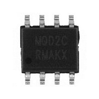
MC9S08QD2CSC Freescale, MC9S08QD2CSC Datasheet - Page 22

MC9S08QD2CSC
Manufacturer Part Number
MC9S08QD2CSC
Description
Manufacturer
Freescale
Datasheet
1.MC9S08QD2CSC.pdf
(198 pages)
Specifications of MC9S08QD2CSC
Cpu Family
HCS08
Device Core Size
8b
Frequency (max)
8MHz
Total Internal Ram Size
128Byte
# I/os (max)
4
Number Of Timers - General Purpose
3
Operating Supply Voltage (typ)
3.3/5V
Operating Supply Voltage (max)
5.5V
Operating Supply Voltage (min)
2.7V
On-chip Adc
4-chx10-bit
Instruction Set Architecture
CISC
Operating Temp Range
-40C to 85C
Operating Temperature Classification
Industrial
Mounting
Surface Mount
Pin Count
8
Package Type
SOIC N
Program Memory Type
Flash
Program Memory Size
2KB
Lead Free Status / RoHS Status
Compliant
Available stocks
Company
Part Number
Manufacturer
Quantity
Price
Part Number:
MC9S08QD2CSC
Manufacturer:
FREESCALE
Quantity:
20 000
Company:
Part Number:
MC9S08QD2CSCR
Manufacturer:
FREESCALE
Quantity:
310
Chapter 2 External Signal Description
Although the BKGD pin is a pseudo open-drain pin, the background debug communication protocol
provides brief, actively driven, high speedup pulses to ensure fast rise times. Small capacitances from
cables and the absolute value of the internal pullup device play almost no role in determining rise and fall
times on the BKGD pin.
2.2.5
The MC9S08QD4 series of MCUs support up to 4 general-purpose I/O pins, 1 input-only pin and 1
output-only pin, which are shared with on-chip peripheral functions (timers, serial I/O, ADC, keyboard
interrupts, etc.). On each of the MC9S08QD4 series devices there is one input-only and one output-only
port pin.
When a port pin is configured as a general-purpose output or a peripheral uses the port pin as an output,
software can select one of two drive strengths and enable or disable slew rate control. When a port pin is
configured as a general-purpose input or a peripheral uses the port pin as an input, software can enable a
pullup device.
For information about controlling these pins as general-purpose I/O pins, see the
Input/Output
see the appropriate chapter referenced in
Immediately after reset, all pins that are not output-only are configured as high-impedance,
general-purpose inputs with internal pullup devices disabled. After reset, the output-only port function is
not enabled but is configured for low output drive strength with slew rate control enabled. The PTA4 pin
defaults to BKGD/MS on any reset.
2.2.5.1
To select drive strength or enable slew rate control or pullup devices, the user writes to the appropriate pin
control register located in the high-page register block of the memory map. The pin control registers
operate independently of the parallel I/O registers and allow control of a port on an individual pin basis.
2.2.5.1.1
An internal pullup device can be enabled for each port pin by setting the corresponding bit in one of the
pullup enable registers (PTxPEn). The pullup device is disabled if the pin is configured as an output by the
parallel I/O control logic or any shared peripheral function, regardless of the state of the corresponding
pullup enable register bit. The pullup device is also disabled if the pin is controlled by an analog function.
The KBI module and IRQ function when enabled for rising edge detection causes an enabled internal pull
device to be configured as a pulldown.
22
General-Purpose I/O and Peripheral Ports
Control.”
Pin Control Registers
To avoid extra current drain from floating input pins, the reset initialization
routine in the application program must either enable on-chip pullup devices
or change the direction of unused pins to outputs so the pins do not float.
Internal Pullup Enable
For information about how and when on-chip peripheral systems use these pins,
MC9S08QD4 Series MCU Data Sheet, Rev. 6
Table
2-1.
NOTE
Chapter 6, “Parallel
Freescale Semiconductor


