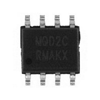
MC9S08QD2CSC Freescale, MC9S08QD2CSC Datasheet - Page 124

MC9S08QD2CSC
Manufacturer Part Number
MC9S08QD2CSC
Description
Manufacturer
Freescale
Datasheet
1.MC9S08QD2CSC.pdf
(198 pages)
Specifications of MC9S08QD2CSC
Cpu Family
HCS08
Device Core Size
8b
Frequency (max)
8MHz
Total Internal Ram Size
128Byte
# I/os (max)
4
Number Of Timers - General Purpose
3
Operating Supply Voltage (typ)
3.3/5V
Operating Supply Voltage (max)
5.5V
Operating Supply Voltage (min)
2.7V
On-chip Adc
4-chx10-bit
Instruction Set Architecture
CISC
Operating Temp Range
-40C to 85C
Operating Temperature Classification
Industrial
Mounting
Surface Mount
Pin Count
8
Package Type
SOIC N
Program Memory Type
Flash
Program Memory Size
2KB
Lead Free Status / RoHS Status
Compliant
Available stocks
Company
Part Number
Manufacturer
Quantity
Price
Part Number:
MC9S08QD2CSC
Manufacturer:
FREESCALE
Quantity:
20 000
Company:
Part Number:
MC9S08QD2CSCR
Manufacturer:
FREESCALE
Quantity:
310
- Current page: 124 of 198
- Download datasheet (3Mb)
Internal Clock Source (S08ICSV1)
9.1.3.5
In FLL bypassed external mode, the FLL is enabled and controlled by an external reference clock, but is
bypassed. The ICS supplies a clock derived from the external reference clock. The external reference clock
can be an external crystal/resonator supplied by an OSC controlled by the ICS, or it can be another external
clock source. The BDC clock is supplied from the FLL.
9.1.3.6
In FLL bypassed external low power mode, the FLL is disabled and bypassed, and the ICS supplies a clock
derived from the external reference clock. The external reference clock can be an external crystal/resonator
supplied by an OSC controlled by the ICS, or it can be another external clock source. The BDC clock is
not available.
9.1.3.7
In stop mode the FLL is disabled and the internal or external reference clocks can be selected to be enabled
or disabled. The BDC clock is not available and the ICS does not provide an MCU clock source.
9.1.4
Figure 9-2
124
is the ICS block diagram.
Block Diagram
RANGE
FLL Bypassed Externa
FLL Bypassed Externa
Stop (STOP)
HGO
IREFS
Figure 9-2. Internal Clock Source (ICS) Block Diagram
External Reference
Clock Source
n=0-7
RDIV
/ 2
Optional
Block
n
MC9S08QD4 Series MCU Data Sheet, Rev. 6
IREFSTEN
Reference
Internal
RDIV_CLK
TRIM
Clock
9
l (FBE)
l Low Power (FBELP)
EREFSTEN
EREFS
Filter
DCO
LP
FLL
ERCLKEN
IRCLKEN
9
Internal Clock Source Block
CLKS
DCOOUT
n=0-3
BDIV
/ 2
/ 2
n
ICSERCLK
ICSIRCLK
ICSOUT
ICSLCLK
ICSFFCLK
Freescale Semiconductor
Related parts for MC9S08QD2CSC
Image
Part Number
Description
Manufacturer
Datasheet
Request
R

Part Number:
Description:
TOWER ELEVATOR BOARDS HARDWARE
Manufacturer:
Freescale Semiconductor
Datasheet:

Part Number:
Description:
TOWER SERIAL I/O HARDWARE
Manufacturer:
Freescale Semiconductor
Datasheet:

Part Number:
Description:
LCD MODULE FOR TWR SYSTEM
Manufacturer:
Freescale Semiconductor
Datasheet:

Part Number:
Description:
DAUGHTER LCD WVGA I.MX51
Manufacturer:
Freescale Semiconductor
Datasheet:

Part Number:
Description:
TOWER SYSTEM BOARD MPC5125
Manufacturer:
Freescale Semiconductor
Datasheet:

Part Number:
Description:
KIT EVALUATION I.MX51
Manufacturer:
Freescale Semiconductor
Datasheet:

Part Number:
Description:
KIT DEVELOPMENT WINCE IMX25
Manufacturer:
Freescale Semiconductor
Datasheet:

Part Number:
Description:
TOWER SYSTEM KIT MPC5125
Manufacturer:
Freescale Semiconductor
Datasheet:

Part Number:
Description:
TOWER SYSTEM BOARD K40X256
Manufacturer:
Freescale Semiconductor
Datasheet:

Part Number:
Description:
TOWER SYSTEM KIT K40X256
Manufacturer:
Freescale Semiconductor
Datasheet:

Part Number:
Description:
Microcontrollers (MCU) MX28 PLATFORM DEV KIT
Manufacturer:
Freescale Semiconductor
Datasheet:

Part Number:
Description:
MCU, MPU & DSP Development Tools IAR KickStart Kit for Kinetis K60
Manufacturer:
Freescale Semiconductor
Datasheet:

Part Number:
Description:
24BIT HDMI MX535/08
Manufacturer:
Freescale Semiconductor
Datasheet:
Part Number:
Description:
Manufacturer:
Freescale Semiconductor, Inc
Datasheet:
Part Number:
Description:
Manufacturer:
Freescale Semiconductor, Inc
Datasheet:


