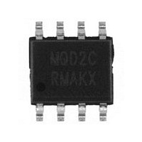
MC9S08QD2CSC Freescale, MC9S08QD2CSC Datasheet - Page 106

MC9S08QD2CSC
Manufacturer Part Number
MC9S08QD2CSC
Description
Manufacturer
Freescale
Datasheet
1.MC9S08QD2CSC.pdf
(198 pages)
Specifications of MC9S08QD2CSC
Cpu Family
HCS08
Device Core Size
8b
Frequency (max)
8MHz
Total Internal Ram Size
128Byte
# I/os (max)
4
Number Of Timers - General Purpose
3
Operating Supply Voltage (typ)
3.3/5V
Operating Supply Voltage (max)
5.5V
Operating Supply Voltage (min)
2.7V
On-chip Adc
4-chx10-bit
Instruction Set Architecture
CISC
Operating Temp Range
-40C to 85C
Operating Temperature Classification
Industrial
Mounting
Surface Mount
Pin Count
8
Package Type
SOIC N
Program Memory Type
Flash
Program Memory Size
2KB
Lead Free Status / RoHS Status
Compliant
Available stocks
Company
Part Number
Manufacturer
Quantity
Price
Part Number:
MC9S08QD2CSC
Manufacturer:
FREESCALE
Quantity:
20 000
Company:
Part Number:
MC9S08QD2CSCR
Manufacturer:
FREESCALE
Quantity:
310
- Current page: 106 of 198
- Download datasheet (3Mb)
Analog-to-Digital Converter (S08ADC10V1)
8.3.9
APCTL2 is used to control channels 8–15 of the ADC module.
106
ADPC15
ADPC14
ADPC13
ADPC12
ADPC11
ADPC10
ADPC1
ADPC0
Field
Field
7
6
5
4
3
2
1
0
Reset:
W
ADC Pin Control 15 — ADPC15 is used to control the pin associated with channel AD15.
0 AD15 pin I/O control enabled
1 AD15 pin I/O control disabled
ADC Pin Control 14 — ADPC14 is used to control the pin associated with channel AD14.
0 AD14 pin I/O control enabled
1 AD14 pin I/O control disabled
ADC Pin Control 13 — ADPC13 is used to control the pin associated with channel AD13.
0 AD13 pin I/O control enabled
1 AD13 pin I/O control disabled
ADC Pin Control 12 — ADPC12 is used to control the pin associated with channel AD12.
0 AD12 pin I/O control enabled
1 AD12 pin I/O control disabled
ADC Pin Control 11 — ADPC11 is used to control the pin associated with channel AD11.
0 AD11 pin I/O control enabled
1 AD11 pin I/O control disabled
ADC Pin Control 10 — ADPC10 is used to control the pin associated with channel AD10.
0 AD10 pin I/O control enabled
1 AD10 pin I/O control disabled
R
Pin Control 2 Register (APCTL2)
ADC Pin Control 1 — ADPC1 is used to control the pin associated with channel AD1.
0 AD1 pin I/O control enabled
1 AD1 pin I/O control disabled
ADC Pin Control 0 — ADPC0 is used to control the pin associated with channel AD0.
0 AD0 pin I/O control enabled
1 AD0 pin I/O control disabled
ADPC15
7
0
Table 8-9. APCTL1 Register Field Descriptions (continued)
ADPC14
0
Table 8-10. APCTL2 Register Field Descriptions
6
Figure 8-12. Pin Control 2 Register (APCTL2)
MC9S08QD4 Series MCU Data Sheet, Rev. 6
ADPC13
0
5
ADPC12
0
4
Description
Description
ADPC11
0
3
ADPC10
0
2
ADPC9
Freescale Semiconductor
0
1
ADPC8
0
0
Related parts for MC9S08QD2CSC
Image
Part Number
Description
Manufacturer
Datasheet
Request
R

Part Number:
Description:
TOWER ELEVATOR BOARDS HARDWARE
Manufacturer:
Freescale Semiconductor
Datasheet:

Part Number:
Description:
TOWER SERIAL I/O HARDWARE
Manufacturer:
Freescale Semiconductor
Datasheet:

Part Number:
Description:
LCD MODULE FOR TWR SYSTEM
Manufacturer:
Freescale Semiconductor
Datasheet:

Part Number:
Description:
DAUGHTER LCD WVGA I.MX51
Manufacturer:
Freescale Semiconductor
Datasheet:

Part Number:
Description:
TOWER SYSTEM BOARD MPC5125
Manufacturer:
Freescale Semiconductor
Datasheet:

Part Number:
Description:
KIT EVALUATION I.MX51
Manufacturer:
Freescale Semiconductor
Datasheet:

Part Number:
Description:
KIT DEVELOPMENT WINCE IMX25
Manufacturer:
Freescale Semiconductor
Datasheet:

Part Number:
Description:
TOWER SYSTEM KIT MPC5125
Manufacturer:
Freescale Semiconductor
Datasheet:

Part Number:
Description:
TOWER SYSTEM BOARD K40X256
Manufacturer:
Freescale Semiconductor
Datasheet:

Part Number:
Description:
TOWER SYSTEM KIT K40X256
Manufacturer:
Freescale Semiconductor
Datasheet:

Part Number:
Description:
Microcontrollers (MCU) MX28 PLATFORM DEV KIT
Manufacturer:
Freescale Semiconductor
Datasheet:

Part Number:
Description:
MCU, MPU & DSP Development Tools IAR KickStart Kit for Kinetis K60
Manufacturer:
Freescale Semiconductor
Datasheet:

Part Number:
Description:
24BIT HDMI MX535/08
Manufacturer:
Freescale Semiconductor
Datasheet:
Part Number:
Description:
Manufacturer:
Freescale Semiconductor, Inc
Datasheet:
Part Number:
Description:
Manufacturer:
Freescale Semiconductor, Inc
Datasheet:


