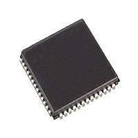
IDT7130SA55JG IDT, Integrated Device Technology Inc, IDT7130SA55JG Datasheet - Page 13

IDT7130SA55JG
Manufacturer Part Number
IDT7130SA55JG
Description
Manufacturer
IDT, Integrated Device Technology Inc
Datasheet
1.IDT7130SA55JG.pdf
(19 pages)
Specifications of IDT7130SA55JG
Density
8Kb
Access Time (max)
55ns
Sync/async
Asynchronous
Architecture
Not Required
Clock Freq (max)
Not RequiredMHz
Operating Supply Voltage (typ)
5V
Address Bus
20b
Package Type
PLCC
Operating Temp Range
0C to 70C
Number Of Ports
2
Supply Current
155mA
Operating Supply Voltage (min)
4.5V
Operating Supply Voltage (max)
5.5V
Operating Temperature Classification
Commercial
Mounting
Surface Mount
Pin Count
52
Word Size
8b
Number Of Words
1K
Lead Free Status / RoHS Status
Compliant
DATA
Timing Waveform of Write with Port-to-Port Read and BUSY
NOTES:
1. To ensure that the earlier of the two ports wins. t
2. CE
3. OE = V
4. All timing is the same for the left and right ports. Port 'A' may be either the left or right port. Port "B" is opposite from port "A".
Timing Waveform of Write with BUSY
NOTES:
1. t
2. BUSY is asserted on port "B" blocking R/W
3. All timing is the same for the left and right ports. Port "A" may be either the left or right port. Port "B" is oppsite from port "A".
DATA
IDT7130SA/LA and IDT7140SA/LA
High-Speed 1K x 8 Dual-Port Static SRAM
ADDR
BUSY
WH
ADDR
R/ W
OUT"B"
L
must be met for both BUSY Input (IDT7140, slave) or Output (IDT7130 master).
= CE
IN"A"
"B"
"B"
"A "
IL
"A"
for the reading port.
R
= V
IL
BUSY
R/W
R/W
"B"
"B"
"A"
t
APS
(1)
"B"
, until BUSY
BDD
is ignored for slave (IDT7140).
"B"
t
goes HIGH.
BAA
t
WB
MATCH
t
WC
13
(2)
t
WP
(3)
t
WP
Military, Industrial and Commercial Temperature Ranges
MATCH
t
VALID
DW
t
BDA
t
WDD
t
WH
(1)
t
DDD
2689 drw 13
t
DH
t
BDD
(2,3,4)
,
VALID
2689 drw 12


