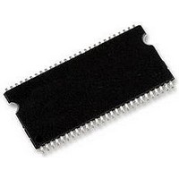
MT48LC16M16A2P-75:D Micron Technology Inc, MT48LC16M16A2P-75:D Datasheet - Page 31

MT48LC16M16A2P-75:D
Manufacturer Part Number
MT48LC16M16A2P-75:D
Description
IC, SDRAM, 256MBIT, 133MHZ, TSOP-54
Manufacturer
Micron Technology Inc
Type
SDRAMr
Series
-r
Specifications of MT48LC16M16A2P-75:D
Organization
16Mx16
Density
256Mb
Address Bus
15b
Access Time (max)
6/5.4ns
Maximum Clock Rate
133MHz
Operating Supply Voltage (typ)
3.3V
Package Type
TSOP-II
Operating Temp Range
0C to 70C
Operating Supply Voltage (max)
3.6V
Operating Supply Voltage (min)
3V
Supply Current
135mA
Pin Count
54
Mounting
Surface Mount
Operating Temperature Classification
Commercial
Memory Type
DRAM - Sychronous
Memory Configuration
16 X 16
Access Time
5.4ns
Page Size
256Mbit
Memory Case Style
TSOP
No. Of Pins
54
Operating Temperature Range
0°C To +70°C
Format - Memory
RAM
Memory Size
256M (16Mx16)
Speed
133MHz
Interface
Parallel
Voltage - Supply
3 V ~ 3.6 V
Operating Temperature
0°C ~ 70°C
Package / Case
54-TSOP (0.400", 10.16mm Width)
Lead Free Status / RoHS Status
Compliant
Lead Free Status / RoHS Status
Compliant, Lead free / RoHS Compliant
Available stocks
Company
Part Number
Manufacturer
Quantity
Price
Company:
Part Number:
MT48LC16M16A2P-75:D
Manufacturer:
SAMTEC
Quantity:
1 200
Company:
Part Number:
MT48LC16M16A2P-75:D
Manufacturer:
MICRON
Quantity:
5 520
Company:
Part Number:
MT48LC16M16A2P-75:D
Manufacturer:
MICRON
Quantity:
6 000
Company:
Part Number:
MT48LC16M16A2P-75:D
Manufacturer:
MICRON42
Quantity:
175
Part Number:
MT48LC16M16A2P-75:D
Manufacturer:
MICRON
Quantity:
20 000
Functional Description
PDF: 09005aef8091e6d1
256Mb_sdr.pdf - Rev. N 1/10 EN
In general, 256Mb SDRAM devices (16 Meg x 4 x 4 banks, 8 Meg x 8 x 4 banks, and 4 Meg
x 16 x 4 banks) are quad-bank DRAM that operate at 3.3V and include a synchronous
interface. All signals are registered on the positive edge of the clock signal, CLK. Each of
the x4’s 67,108,864-bit banks is organized as 8192 rows by 2048 columns by 4 bits. Each
of the x8’s 67,108,864-bit banks is organized as 8192 rows by 1024 columns by 8 bits.
Each of the x16’s 67,108,864-bit banks is organized as 8192 rows by 512 columns by 16
bits.
Read and write accesses to the SDRAM are burst-oriented; accesses start at a selected
location and continue for a programmed number of locations in a programmed se-
quence. Accesses begin with the registration of an ACTIVE command, followed by a
READ or WRITE command. The address bits registered coincident with the ACTIVE com-
mand are used to select the bank and row to be accessed (BA0 and BA1 select the bank,
A[12:0] select the row). The address bits (x4: A[9:0], A11; x8: A[9:0]; x16: A[8:0]) registered
coincident with the READ or WRITE command are used to select the starting column
location for the burst access.
Prior to normal operation, the SDRAM must be initialized. The following sections pro-
vide detailed information covering device initialization, register definition, command
descriptions, and device operation.
31
Micron Technology, Inc. reserves the right to change products or specifications without notice.
256Mb: x4, x8, x16 SDRAM
Functional Description
© 1999 Micron Technology, Inc. All rights reserved.


