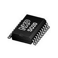
SA5217D NXP Semiconductors, SA5217D Datasheet - Page 8

SA5217D
Manufacturer Part Number
SA5217D
Description
Manufacturer
NXP Semiconductors
Datasheet
1.SA5217D.pdf
(12 pages)
Specifications of SA5217D
Operating Temperature (min)
-40C
Operating Temperature (max)
85C
Operating Temperature Classification
Industrial
Mounting
Surface Mount
Pin Count
20
Lead Free Status / RoHS Status
Compliant
Available stocks
Company
Part Number
Manufacturer
Quantity
Price
Part Number:
SA5217D
Manufacturer:
PHILIPS/飞利浦
Quantity:
20 000
Philips Semiconductors
For more information on this application, please refer to Application
Brief AB1432.
Die Sales Disclaimer
Due to the limitations in testing high frequency and other parameters
at the die level, and the fact that die electrical characteristics may
shift after packaging, die electrical parameters are not specified and
die are not guaranteed to meet electrical characteristics (including
temperature range) as noted in this data sheet which is intended
only to specify electrical characteristics for a packaged device.
All die are 100% functional with various parametrics tested at the
wafer level, at room temperature only (25 C), and are guaranteed to
be 100% functional as a result of electrical testing to the point of
wafer sawing only. Although the most modern processes are
1998 Oct 07
Postamplifier with link status indicator
10 H
NOTE:
THE NE5210/NE5217 combination can operate at data rates in excess of 100Mb/s NRZ
L3
10 H
L2
C13
10 F
C15
10 F
220
R2
.01 F
C11
R3
33k
C12
.01 F
100pF
C14
LED
D1
V
OUT
(TTL)
10
1
2
3
4
5
6
7
8
9
THRESH
LED
C
GND
FLAG
JAM
V
V
GND
TTL
PKDET
CCD
CCA
OUT
A
D
Figure 6. A 50Mb/s Fiber Optic Receiver
R
R
PKDET
OUT
OUT
C
C
HYST
IN
IN
IN
IN
AZP
AZN
C1
C2
1B
1A
2B
8B
2A
8A
+V
18
16
CC
20
19
17
15
14
13
12
11
R5
10k
C7
0.1 F
0.1 F
47 F
.01 F
C8
C9
0.1 F
100pF
C10
8
utilized for wafer sawing and die pick and place into waffle pack
carriers, it is impossible to guarantee 100% functionality through this
process. There is no post waffle pack testing performed on
individual die.
Since Philips Semiconductors has no control of third party
procedures in the handling or packaging of die, Philips
Semiconductors assumes no liability for device functionality or
performance of the die or systems on any die sales.
Although Philips Semiconductors typically realizes a yield of 85%
after assembling die into their respective packages, with care
customers should achieve a similar yield. However, for the reasons
stated above, Philips Semiconductors cannot guarantee this or any
other yield on any die sales.
GND
R4
4k
10
11
12
13
14
8
9
GND
GND
GND
GND
OUT
GND
OUT
1
2
V
V
GND
GND
CC1
CC2
NC
I
NC
IN
1
7
6
5
4
3
2
.01 F
C4
10 H
L1
Product specification
SA5217
10 F
R1
100
C3
OPTICAL
BPF31
INPUT
SD00359
1.0 F
.01 F
C5
C6


