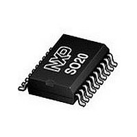
SA5217D NXP Semiconductors, SA5217D Datasheet - Page 3

SA5217D
Manufacturer Part Number
SA5217D
Description
Manufacturer
NXP Semiconductors
Datasheet
1.SA5217D.pdf
(12 pages)
Specifications of SA5217D
Operating Temperature (min)
-40C
Operating Temperature (max)
85C
Operating Temperature Classification
Industrial
Mounting
Surface Mount
Pin Count
20
Lead Free Status / RoHS Status
Compliant
Available stocks
Company
Part Number
Manufacturer
Quantity
Price
Part Number:
SA5217D
Manufacturer:
PHILIPS/飞利浦
Quantity:
20 000
Philips Semiconductors
PIN DESCRIPTIONS
BLOCK DIAGRAM
1998 Oct 07
NO.
PIN
10
12
13
14
15
16
17
18
19
20
11
Postamplifier with link status indicator
1
2
3
4
5
6
7
8
9
SYMBOL
LED
C
THRESH
GND
FLAG
JAM
V
V
GND
V
R
R
IN
OUT
IN
OUT
C
C
IN
IN
CCD
CCA
OUT
PKDET
PKDET
HYST
AZN
AZP
8A
8B
1A
1B
2A
2B
A
D
R
Output for the LED driver. Open collector output transistor with 125 series limiting resistor. An above threshold signal
turns this transistor ON.
Capacitor for the peak detector. The value of this capacitor determines the detector response time to the signal, supple-
menting the internal 10pF capacitor.
Peak detector threshold resistor. The value of this resistor determines the threshold level of the peak detector.
Device analog ground pin.
Peak detector digital output. When this output is LOW, there is data present above the threshold. This pin is normally
connected to the JAM pin and has a TTL fanout of two.
Input to inhibit data flow. Sending the pin HIGH forces TTL DATA OUT ON, Pin 10, LOW. This pin is normally connected
to the FLAG pin and is TTL-compatible.
Power supply pin for the digital portion of the chip.
Power supply pin for the analog portion of the chip.
Device digital ground pin.
TTL output pin with a fanout of five.
Peak detector current resistor. The value of this resistor determines the amount of discharge current available to the
peak detector capacitor, C
Peak detector hysteresis resistor. The value of this resistor determines the amount of hysteresis in the peak detector.
Non-inverting input to amplifier A8.
Non-inverting output of amplifier A2.
Inverting input to amplifier A8.
Inverting output of amplifier A2.
Auto-Zero capacitor pin (Negative terminal). The value of this capacitor determines the low-end frequency response of
the preamp A1.
Auto-Zero capacitor pin (Positive terminal). The value of this capacitor determines the low-end frequency response of the
preamp A1.
Non-inverting input of the preamp A1.
Inverting input of the preamp A1.
PKDET
C
C
IN
IN
AZP
AZN
1B
1A
20
19
18
17
11
GND
A1
4
A
GND
9
D
V
PKDET
CCA
8
THRESH
3
.
PEAK DETECT
Figure 2. Block Diagram
A3
A2
GATED AMP
V
CCD
7
C
2
PKDET
3
DESCRIPTION
OUT
2A
14
OUT
HYSTERESIS
16
A4
2B
A6
A7
IN
12
OUTPUT DISABLE
8B
R
HYST
15
LED DRIVER
IN
13
A5
8A
A8
SCHMITT TRIGGER
10
6
5
1
SD00355
V
JAM
FLAG
LED
OUT
Product specification
SA5217


