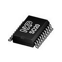
SA5217D NXP Semiconductors, SA5217D Datasheet - Page 7

SA5217D
Manufacturer Part Number
SA5217D
Description
Manufacturer
NXP Semiconductors
Datasheet
1.SA5217D.pdf
(12 pages)
Specifications of SA5217D
Operating Temperature (min)
-40C
Operating Temperature (max)
85C
Operating Temperature Classification
Industrial
Mounting
Surface Mount
Pin Count
20
Lead Free Status / RoHS Status
Compliant
Available stocks
Company
Part Number
Manufacturer
Quantity
Price
Part Number:
SA5217D
Manufacturer:
PHILIPS/飞利浦
Quantity:
20 000
Philips Semiconductors
TYPICAL PERFORMANCE CHARACTERISTICS (continued)
THEORY OF OPERATION AND APPLICATION
The SA5217 postamplifier is a highly integrated chip that provides
up to 60dB of gain at 60MHz, to bring mV level signals up to TTL
levels.
The SA5217 contains eight amplifier blocks (see Block Diagram).
The main signal path is made up of a cascade of limiting stages: A1,
A2 and A8. The A3-A4-A7 path performs a wideband full-wave
rectification of the input signal with adjustable hysteresis and decay
times. It outputs a TTL High on the “FLAG” output (Pin 5) when the
input is below a user adjustable threshold. An on-chip LED driver
turns the external LED to the On state when the input signal is
above the threshold. In a typical application the “FLAG” output is
tied back tot he “JAM” input; forcing the “JAM” input to TTL High will
latch the TTL Data Out at the last logical state.
Threshold voltage and hysteresis voltage range are adjustable with
resistors R
sheet will result in performance shown in the graph “Hysteresis and
Forward Active Region”. A minority of parts may be sensitive
enough that FLAG High (Off) occurs below the minimum functional
1998 Oct 07
Postamplifier with link status indicator
16
14
12
10
6
4
2
8
10
40
35
25
20
15
Hysteresis vs R
45
30
10
Threshold vs R
V
T
F = 60MHz
2k
THRESH
A
CC
= 27 C
= 5V
5k
3k
6k
and R
20
(Driven Single Ended)
THRESH
20
4k
HYST
(Driven Single Ended)
THRESH
5k
. The typical values given in the data
R
2k
THRESH
for Different Values of R
3k
R
for Different Values of R
30
THRESH
4k
6k
30
(k )
(k )
Figure 5. Typical Performance Characteristics (cont)
40
40
V
T
F = 60MHz
A
CC
HYST
= 27 C
HYST
= 5V
50
50
7
input signal level, V
the graph. Such parts may require adjustment of R
important to guarantee that an output signal is present for the full
hysteresis range. If this is not important, R
to give a FLAG Low for lower level input signals.
An auto-zero loop allows the SA5217 to be directly connected to a
transimpedance amplifier such as the SA5210, SA5211, or
SA5212A without coupling capacitors. This auto-zero loop cancels
the transimpedance amplifier’s DC offset, the SA5217 A1 offset, and
the data-dependent offset in the PIN diode/transimpedance amplifier
combination.
A typical application of the SA5217 postamplifier is depicted in
Figure 6. The system uses the SA5211 transimpedance amplifier
which has a 28k differential transimpedance gain and a -3dB
bandwidth of 140MHz. this typical application is optimized for a
50Mb/s Non Return to Zero (NRZ) bit stream.
As the system’s gain bandwidth product is very high, it is crucial to
employ good RF design and printed circuit board layout techniques
to prevent the system from becoming unstable.
40
30
20
10
50
0
10
On/Off Voltage vs R
OFF
0N
0
4
3
2
5
1
0
Hysteresis and Forward Active Region
20
IN1
. This condition is shown by the dotted line in
5
OFF
V
IN1
THRESH
R
ON
THRESH
10
30
V
V
IN
HYS
(Driven Single Ended)
15
(mV
(k )
P-P
THRESH
R
R
THRESH
HYST
)
20
V
Product specification
40
THR
FORWARD
(shaded)
REGION
ACTIVE
= 4k
V
T
F = 60MHz
R
may be adjusted
THRESH
SA5217
A
CC
HYST
= 33k
25
= 27 C
= 5V
SD00358
= 4k
30
if it is
50


