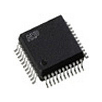
SAA7120H/V2,557 NXP Semiconductors, SAA7120H/V2,557 Datasheet - Page 17

SAA7120H/V2,557
Manufacturer Part Number
SAA7120H/V2,557
Description
Manufacturer
NXP Semiconductors
Datasheet
1.SAA7120HV2557.pdf
(36 pages)
Specifications of SAA7120H/V2,557
Adc/dac Resolution
10b
Screening Level
Commercial
Package Type
PQFP
Pin Count
44
Lead Free Status / RoHS Status
Compliant
Philips Semiconductors
Table 21 Subaddresses 63H to 66H (four bytes to program subcarrier frequency)
Note
1. Examples:
Table 22 Subaddresses 67H to 6AH
Table 23 Subaddress 6BH
2002 Oct 11
FSC0 to
FSC3
L21O0
L21O1
L21E0
L21E1
PRCV2
ORCV2
CBLF
PRCV1
ORCV1
TRCV2
SRCV1
DATA BYTE
DATA BYTE
DATA BYTE
Digital video encoder
a) NTSC-M: f
b) PAL-B/G: f
f
multiples of line frequency);
f
multiples of line frequency)
first byte of captioning data, odd field
second byte of captioning data, odd field
first byte of extended data, even field
second byte of extended data, even field
LOGIC
LEVEL
sc
llc
sc
sc
= clock frequency (in
= subcarrier frequency (in
0
1
0
1
0
1
0
1
0
1
0
1
= 227.5, f
= 283.7516, f
DESCRIPTION
polarity of RCV2 as output is active HIGH, rising edge is taken when input, respectively;
default after reset
polarity of RCV2 as output is active LOW, falling edge is taken when input, respectively
pin RCV2 is switched to input; default after reset
pin RCV2 is switched to output
if ORCV2 = HIGH, pin RCV2 provides an HREF signal (horizontal reference pulse that is
defined by RCV2S and RCV2E, also during vertical blanking interval); default after reset
if ORCV2 = LOW and bit SYMP = LOW, signal input to RCV2 is used for horizontal
synchronization only (if TRCV2 = 1); default after reset
if ORCV2 = HIGH, pin RCV2 provides a ‘composite-blanking-not’ signal, for example a
reference pulse that is defined by RCV2S and RCV2E, excluding vertical blanking interval,
which is defined by FAL and LAL
if ORCV2 = LOW and bit SYMP = LOW, signal input to RCV2 is used for horizontal
synchronization (if TRCV2 = 1) and as an internal blanking signal
polarity of RCV1 as output is active HIGH, rising edge is taken when input; default after reset
polarity of RCV1 as output is active LOW, falling edge is taken when input
pin RCV1 is switched to input; default after reset
pin RCV1 is switched to output
horizontal synchronization is taken from RCV1 port (at bit SYMP = LOW) or from decoded
frame sync of “ CCIR 656” input (at bit SYMP = HIGH); default after reset
horizontal synchronization is taken from RCV2 port (at bit SYMP = LOW)
defines signal type on pin RCV1; see Table 24
llc
= 1716
DESCRIPTION
llc
= 1728
FSC = 569408543 (21F07C1FH).
FSC = 705268427 (2A098ACBH).
note 1
FSC
=
17
round
CONDITIONS
DESCRIPTION
f
------
f
llc
sc
LSBs of the respective bytes are encoded
immediately after run-in and framing code, the
MSBs of the respective bytes have to carry the
parity bit, in accordance with the definition of
line 21 encoding format
2
32
;
SAA7120H; SAA7121H
FSC3 = most significant byte;
FSC0 = least significant byte
REMARKS
REMARKS
Product specification


