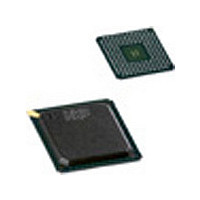
SAA7118EEB-T NXP Semiconductors, SAA7118EEB-T Datasheet - Page 65

SAA7118EEB-T
Manufacturer Part Number
SAA7118EEB-T
Description
Video ICs COMPONENT VID DECODER W/COMB F
Manufacturer
NXP Semiconductors
Type
Multi-Standard Video Decoderr
Datasheet
1.SAA7118EEB-T.pdf
(177 pages)
Specifications of SAA7118EEB-T
Adc/dac Resolution
9b
Screening Level
Commercial
Package Type
LBGA
Pin Count
156
Maximum Operating Temperature
+ 70 C
Package / Case
SOT-700
Minimum Operating Temperature
0 C
Mounting Style
SMD/SMT
Lead Free Status / RoHS Status
Not Compliant
Other names
SAA7118E/V1,518
- Current page: 65 of 177
- Download datasheet (906Kb)
NXP Semiconductors
Table 19.
[1]
[2]
SAA7118_7
Product data sheet
Event description
Next pixel is FIRST pixel of any
active line
Previous pixel was LAST pixel of
any active line, but not the last
Next pixel is FIRST pixel of any
V-blanking line
Previous pixel was LAST pixel of
the last active line or of any
V-blanking line
No valid data, don’t capture and
don’t increment pointer
The leading byte sequence is: FFh-00h-00h.
The MSB of the SAV/EAV code byte is controlled by:
a) Scaler output data: task A
b) VBI data slicer output data: DID[5:0] 5Dh[5:0] = 3Eh
SAV/EAV codes on I port
8.6.5 Data stream coding and reference signal generation (subaddresses 84h,
85h and 93h)
As H and V reference signals are logic 1, active gate signals are generated, which frame
the transfer of the valid output data. As an alternative to the gates, H and V trigger pulses
are generated on the rising edges of the gates.
Due to the dynamic FIFO behavior of the complete scaler path, the output signal timing
has no fixed timing relationship to the real-time input video stream. So fixed propagation
delays, in terms of clock cycles, related to the analog input cannot be defined.
The data stream is accompanied by a data qualifier. Additionally invalid data cycles are
marked with code 00h.
If ITU 656 like codes are not required, they can be suppressed in the output stream.
As a further option, it is possible to provide the scaler with an external gating signal on
pin ITRDY. Thereby making it possible to hold the data output for a certain time and to get
valid output data in bursts of a guaranteed length.
The sketched reference signals and events can be mapped to the I port output pins IDQ,
IGPH, IGPV, IGP0 and IGP1. For flexible use the polarities of all the outputs can be
modified. The default polarity for the qualifier and reference signals is logic 1 (active).
Table 19
MSB = CONLH[90h[7]]; task B
SAV/EAV codes on I port
MSB
Field ID = 0
0E
13
25
38
00
shows the relevant and supported SAV and EAV coding.
[2]
of SAV/EAV byte = 0
Rev. 07 — 7 July 2008
Field ID = 1
49
54
62
7F
MSB = 1; DID[5:0] 5Dh[5:0] = 3Fh
Multistandard video decoder with adaptive comb filter
[1]
(hexadecimal)
MSB = CONLH[C0h[7]].
MSB
Field ID = 0
80
9D
AB
B6
[2]
of SAV/EAV byte = 1
Field ID = 1
C7
DA
EC
F1
MSB = 0
SAA7118
© NXP B.V. 2008. All rights reserved.
Comment
HREF = active;
VREF = active
HREF = inactive;
VREF = active
HREF = active;
VREF = inactive
HREF = inactive;
VREF = inactive
IDQ pin inactive
65 of 177
Related parts for SAA7118EEB-T
Image
Part Number
Description
Manufacturer
Datasheet
Request
R

Part Number:
Description:
Manufacturer:
NXP Semiconductors
Datasheet:
Part Number:
Description:
Video ICs COMPONENT + VIDEO PROCESSOR
Manufacturer:
NXP Semiconductors

Part Number:
Description:
IC VIDEO DECOD W/FILTER 156LBGA
Manufacturer:
NXP Semiconductors
Datasheet:
Part Number:
Description:
IC VIDEO DECOD W/FILTER 156LBGA
Manufacturer:
NXP Semiconductors

Part Number:
Description:
IC VIDEO DECODER W/FILTER 156BGA
Manufacturer:
NXP Semiconductors

Part Number:
Description:
IC VIDEO DECODR W/FILTER 156LBGA
Manufacturer:
NXP Semiconductors

Part Number:
Description:
IC VIDEO DECODR W/FILTER 156LBGA
Manufacturer:
NXP Semiconductors

Part Number:
Description:
Manufacturer:
NXP Semiconductors
Datasheet:
Part Number:
Description:
Video ICs VIDEO DECODER W/FILTER
Manufacturer:
NXP Semiconductors
Part Number:
Description:
Multistandard Video Decoder With Adaptive Comb Filter And Component Video Input
Manufacturer:
NXP Semiconductors
Datasheet:
Part Number:
Description:
NXP Semiconductors designed the LPC2420/2460 microcontroller around a 16-bit/32-bitARM7TDMI-S CPU core with real-time debug interfaces that include both JTAG andembedded trace
Manufacturer:
NXP Semiconductors
Datasheet:

Part Number:
Description:
NXP Semiconductors designed the LPC2458 microcontroller around a 16-bit/32-bitARM7TDMI-S CPU core with real-time debug interfaces that include both JTAG andembedded trace
Manufacturer:
NXP Semiconductors
Datasheet:
Part Number:
Description:
NXP Semiconductors designed the LPC2468 microcontroller around a 16-bit/32-bitARM7TDMI-S CPU core with real-time debug interfaces that include both JTAG andembedded trace
Manufacturer:
NXP Semiconductors
Datasheet:
Part Number:
Description:
NXP Semiconductors designed the LPC2470 microcontroller, powered by theARM7TDMI-S core, to be a highly integrated microcontroller for a wide range ofapplications that require advanced communications and high quality graphic displays
Manufacturer:
NXP Semiconductors
Datasheet:
Part Number:
Description:
NXP Semiconductors designed the LPC2478 microcontroller, powered by theARM7TDMI-S core, to be a highly integrated microcontroller for a wide range ofapplications that require advanced communications and high quality graphic displays
Manufacturer:
NXP Semiconductors
Datasheet:


