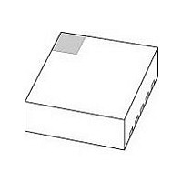
PCA8565BS/1-T NXP Semiconductors, PCA8565BS/1-T Datasheet - Page 4

PCA8565BS/1-T
Manufacturer Part Number
PCA8565BS/1-T
Description
Real Time Clock AUTOMOTIVE CLOCK/CAL
Manufacturer
NXP Semiconductors
Datasheet
1.PCA8565BS1-T.pdf
(39 pages)
Specifications of PCA8565BS/1-T
Bus Type
Serial (2-Wire, I2C)
Operating Supply Voltage (typ)
2.5/3.3/5V
Operating Supply Voltage (max)
5.5V
Operating Supply Voltage (min)
1.8V
Operating Temperature (min)
-40C
Pin Count
10
Mounting
Surface Mount
Date Format
DW:DM:M:Y
Time Format
HH:MM:SS
Mounting Style
SMD/SMT
Package / Case
HVSON
Lead Free Status / RoHS Status
Compliant
Other names
PCA8565BS/1,118
NXP Semiconductors
7. Pinning information
PCA8565_2
Product data sheet
Fig 2.
Top view. For mechanical details see
Pin configuration of PCA8565TS (TSSOP8)
OSCO
OSCI
V
INT
SS
7.1 Pinning
7.2 Pin description
1
2
3
4
PCA8565TS
Table 3.
[1]
Symbol
OSCI
OSCO
n.c.
INT
V
SDA
SCL
CLKOUT
V
SS
DD
The die paddle (exposed pad) is wired to V
001aaj754
Pin description
8
7
6
5
V
CLKOUT
SCL
SDA
DD
Pin
TSSOP8
1
2
-
3
4
5
6
7
8
Figure
28.
Rev. 02 — 16 June 2009
HVSON10
1
2
3, 10
4
5
6
7
8
9
[1]
Fig 3.
SS
Description
oscillator input
oscillator output
do not connect and do not use as feed through;
connect to V
interrupt output (open-drain; active LOW)
ground
serial data I/O
serial clock input
clock output, open-drain
positive supply voltage
but should not be electrically connected.
index area
terminal 1
For mechanical details see
Pin configuration of PCA8565BS (HVSON10)
OSCO
OSCI
V
n.c.
INT
SS
DD
1
2
3
4
5
if floating pins are not allowed
Transparent top view
PCA8565BS
Real time clock/calendar
Figure
001aaj753
PCA8565
29.
© NXP B.V. 2009. All rights reserved.
10
9
8
7
6
n.c.
V
CLKOUT
SCL
SDA
DD
4 of 39


