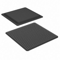
XC3SD3400A-4FGG676C Xilinx Inc, XC3SD3400A-4FGG676C Datasheet - Page 37

XC3SD3400A-4FGG676C
Manufacturer Part Number
XC3SD3400A-4FGG676C
Description
FPGA, SPARTAN-3A, DSP, 676FBGA
Manufacturer
Xilinx Inc
Series
Spartan™-3A DSPr
Datasheets
1.XC3S50A-4VQG100C.pdf
(7 pages)
2.XC3SD3400A-4FGG676C.pdf
(4 pages)
3.XC3SD3400A-4FGG676C.pdf
(101 pages)
Specifications of XC3SD3400A-4FGG676C
No. Of Logic Blocks
5968
No. Of Gates
3400000
No. Of Macrocells
53712
Family Type
Spartan-3A
No. Of Speed Grades
4
Total Ram Bits
2322432
No. Of I/o's
502
Clock Management
DCM
I/o Supply
RoHS Compliant
Number Of Logic Elements/cells
53712
Number Of Labs/clbs
5968
Number Of I /o
469
Number Of Gates
3400000
Voltage - Supply
1.14 V ~ 1.26 V
Mounting Type
Surface Mount
Operating Temperature
0°C ~ 85°C
Package / Case
676-BBGA
Package
676FBGA
Family Name
Spartan®-3A
Device Logic Units
53712
Device System Gates
3400000
Maximum Internal Frequency
667 MHz
Typical Operating Supply Voltage
1.2 V
Maximum Number Of User I/os
469
Ram Bits
2322432
Rohs Compliant
Yes
Lead Free Status / RoHS Status
Lead free / RoHS Compliant
For Use With
122-1532 - KIT DEVELOPMENT SPARTAN 3ADSP
Lead Free Status / RoHS Status
Lead free / RoHS Compliant
Other names
122-1539
Available stocks
Company
Part Number
Manufacturer
Quantity
Price
Company:
Part Number:
XC3SD3400A-4FGG676C
Manufacturer:
XilinxInc
Quantity:
3 000
Company:
Part Number:
XC3SD3400A-4FGG676C
Manufacturer:
Xilinx Inc
Quantity:
10 000
Company:
Part Number:
XC3SD3400A-4FGG676C
Manufacturer:
XILINX
Quantity:
592
Part Number:
XC3SD3400A-4FGG676C
Manufacturer:
XILINX/赛灵思
Quantity:
20 000
Table 28: Recommended Simultaneously Switching
Outputs per V
DS610 (v3.0) October 4, 2010
Product Specification
LVCMOS12
PCI33_3
PCI66_3
HSTL_I
HSTL_III
HSTL_I_18
HSTL_II_18
HSTL_III_18
SSTL18_I
SSTL18_II
SSTL2_I
SSTL2_II
SSTL3_I
SSTL3_II
Signal Standard
(IOSTANDARD)
CCO
QuietIO
/GND Pair (V
Slow
Fast
2
4
6
2
4
6
2
4
6
CCAUX
Top, Bottom
(Banks 0, 2)
40
31
55
16
17
10
18
–
–
–
–
–
–
–
–
–
–
7
–
–
8
6
CS484, FG676
Package Type
= 3.3V) (Cont’d)
Left, Right
(Banks 1, 3)
40
25
18
31
13
55
36
36
16
13
20
17
15
18
10
9
8
5
8
9
9
7
Spartan-3A DSP FPGA Family: DC and Switching Characteristics
www.xilinx.com
Table 28: Recommended Simultaneously Switching
Outputs per V
Notes:
1.
2.
3.
Differential Standards (Number of I/O Pairs or Channels)
LVDS_25
LVDS_33
BLVDS_25
MINI_LVDS_25
MINI_LVDS_33
LVPECL_25
LVPECL_33
RSDS_25
RSDS_33
TMDS_33
PPDS_25
PPDS_33
DIFF_HSTL_I_18
DIFF_HSTL_II_18
DIFF_HSTL_III_18
DIFF_HSTL_I
DIFF_HSTL_III
DIFF_SSTL18_I
DIFF_SSTL18_II
DIFF_SSTL2_I
DIFF_SSTL2_II
DIFF_SSTL3_I
DIFF_SSTL3_II
Not all I/O standards are supported on all I/O banks. The left and
right banks (I/O banks 1 and 3) support higher output drive
current than the top and bottom banks (I/O banks 0 and 2).
Similarly, true differential output standards, such as LVDS,
RSDS, PPDS, miniLVDS, and TMDS, are only supported in top
or bottom banks (I/O banks 0 and 2). Refer to UG331: Spartan-3
Generation FPGA User Guide for additional information.
The numbers in this table are recommendations that assume
sound board lay out practice. This table assumes the following
parasitic factors: combined PCB trace and land inductance per
V
Test limits are the V
standard.
If more than one signal standard is assigned to the I/Os of a
given bank, refer to XAPP689: Managing Ground Bounce in
Large FPGAs for information on how to perform weighted
average SSO calculations.
CCO
Signal Standard
(IOSTANDARD)
and GND pin of 1.0 nH, receiver capacitive load of 15 pF.
CCO
/GND Pair (V
IL
/V
IH
voltage limits for the respective I/O
CCAUX
Top, Bottom
(Banks 0, 2)
22
27
22
27
22
27
27
22
27
4
8
–
5
–
–
3
–
9
–
4
3
CS484, FG676
Package Type
= 3.3V) (Cont’d)
Inputs Only
Inputs Only
Left, Right
(Banks 1, 3)
10
–
–
4
–
–
–
–
–
–
–
8
2
4
4
7
4
9
4
5
3
37


