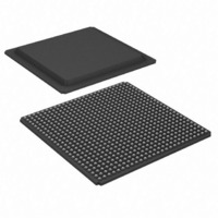
XC3SD3400A-4FGG676C Xilinx Inc, XC3SD3400A-4FGG676C Datasheet - Page 22

XC3SD3400A-4FGG676C
Manufacturer Part Number
XC3SD3400A-4FGG676C
Description
FPGA, SPARTAN-3A, DSP, 676FBGA
Manufacturer
Xilinx Inc
Series
Spartan™-3A DSPr
Datasheets
1.XC3S50A-4VQG100C.pdf
(7 pages)
2.XC3SD3400A-4FGG676C.pdf
(4 pages)
3.XC3SD3400A-4FGG676C.pdf
(101 pages)
Specifications of XC3SD3400A-4FGG676C
No. Of Logic Blocks
5968
No. Of Gates
3400000
No. Of Macrocells
53712
Family Type
Spartan-3A
No. Of Speed Grades
4
Total Ram Bits
2322432
No. Of I/o's
502
Clock Management
DCM
I/o Supply
RoHS Compliant
Number Of Logic Elements/cells
53712
Number Of Labs/clbs
5968
Number Of I /o
469
Number Of Gates
3400000
Voltage - Supply
1.14 V ~ 1.26 V
Mounting Type
Surface Mount
Operating Temperature
0°C ~ 85°C
Package / Case
676-BBGA
Package
676FBGA
Family Name
Spartan®-3A
Device Logic Units
53712
Device System Gates
3400000
Maximum Internal Frequency
667 MHz
Typical Operating Supply Voltage
1.2 V
Maximum Number Of User I/os
469
Ram Bits
2322432
Rohs Compliant
Yes
Lead Free Status / RoHS Status
Lead free / RoHS Compliant
For Use With
122-1532 - KIT DEVELOPMENT SPARTAN 3ADSP
Lead Free Status / RoHS Status
Lead free / RoHS Compliant
Other names
122-1539
Available stocks
Company
Part Number
Manufacturer
Quantity
Price
Company:
Part Number:
XC3SD3400A-4FGG676C
Manufacturer:
XilinxInc
Quantity:
3 000
Company:
Part Number:
XC3SD3400A-4FGG676C
Manufacturer:
Xilinx Inc
Quantity:
10 000
Company:
Part Number:
XC3SD3400A-4FGG676C
Manufacturer:
XILINX
Quantity:
592
Part Number:
XC3SD3400A-4FGG676C
Manufacturer:
XILINX/赛灵思
Quantity:
20 000
Input Setup and Hold Times
Table 19: Setup and Hold Times for the IOB Input Path
DS610 (v3.0) October 4, 2010
Product Specification
Setup Times
T
T
Hold Times
T
Symbol
IOPICK
IOPICKD
IOICKP
Time from the setup of data at the Input
pin to the active transition at the ICLK
input of the Input Flip-Flop (IFF). No Input
Delay is programmed.
Time from the setup of data at the Input
pin to the active transition at the ICLK
input of the Input Flip-Flop (IFF). The
Input Delay is programmed.
Time from the active transition at the
ICLK input of the Input Flip-Flop (IFF) to
the point where data must be held at the
Input pin. No Input Delay is programmed.
Description
LVCMOS25
LVCMOS25
LVCMOS25
Conditions
Spartan-3A DSP FPGA Family: DC and Switching Characteristics
www.xilinx.com
(2)
(2)
(3)
IFD_DELAY_VALUE=0 XC3SD1800A
DELAY_
VALUE
1
2
3
4
5
6
7
8
1
2
3
4
5
6
7
8
0
XC3SD3400A
XC3SD1800A
XC3SD3400A
XC3SD1800A –0.63 –0.52
XC3SD3400A –0.56 –0.56
Device
1.65
1.51
2.09
2.67
3.25
3.75
3.69
4.47
5.27
5.79
2.07
2.57
3.44
4.01
3.89
4.43
5.20
5.70
Min
-5
Speed
1.81
1.88
2.24
2.83
3.64
4.20
4.16
5.09
6.02
6.63
2.44
3.02
3.81
4.39
4.26
5.08
5.95
6.55
Min
-4
Units
ns
ns
ns
ns
ns
ns
ns
ns
ns
ns
ns
ns
ns
ns
ns
ns
ns
ns
ns
ns
22


