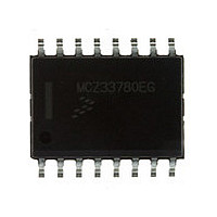
MCZ33780EG Freescale, MCZ33780EG Datasheet - Page 8

MCZ33780EG
Manufacturer Part Number
MCZ33780EG
Description
Manufacturer
Freescale
Datasheet
1.MCZ33780EG.pdf
(37 pages)
Specifications of MCZ33780EG
Operating Supply Voltage (typ)
5/12/15/18/24V
Operating Supply Voltage (min)
4.75/9V
Operating Supply Voltage (max)
5.25/25V
Operating Temp Range
-40C to 85C
Operating Temperature Classification
Industrial
Mounting
Surface Mount
Pin Count
16
Lead Free Status / RoHS Status
Compliant
Available stocks
Company
Part Number
Manufacturer
Quantity
Price
Company:
Part Number:
MCZ33780EG
Manufacturer:
Freescale Semiconductor
Quantity:
135
Company:
Part Number:
MCZ33780EG
Manufacturer:
Freescale
Quantity:
21
Part Number:
MCZ33780EG
Manufacturer:
FREESCALE
Quantity:
20 000
Table 4. Dynamic Electrical Characteristics (continued)
noted. Voltages relative to GND unless otherwise noted. Typical values noted reflect the approximate parameter means at
T
8
33780
ELECTRICAL CHARACTERISTICS
DYNAMIC ELECTRICAL CHARACTERISTICS
BUS TRANSMITTER
Notes
A
Idle-to-Signal and Signal-to-Idle Slew Rate (12 ≤ V
Signal High-to-Low and Signal Low-to-High Slew Rate
(See Data Valid DSIS to DnD Timing)
Communication Data Rate Capability
Valid and Receiver Delay Measurements)
Signal Bit Time (1 / D
INT
INT
INT
INT
DBUS Start Delay,
Data Valid
Signal Driver Overcurrent Shutdown Delay
Signal Low Time for Logic Zero
Signal Low Time for Logic One
10
11
12
13
14
15
16
Characteristics noted under conditions 4.75 V ≤ V
= 25°C under nominal conditions unless otherwise noted.
CS
Spread Spectrum Mode Disabled
Spread Spectrum Mode Enabled
DSIF (
DSIS (MOSI) = 0.5 * V
DSIS (MOSI) = 0.5 * V
DSIF (
33.3% Duty Cycle
66.7% Duty Cycle
Turn ON Delay, DBUS Transaction End to Receive FIFO
Low
Turn ON Delay (C = 100 pF)
Turn OFF Delay,
C = 7.5 nF from DnH to DnL and 4.7 nF from DnH and DnL to GND, capacitor tolerance = ±10%.
In the case where the SPI write to DnL (initiating a DBUS transaction start or causing an interrupt) is the last byte in the burst sequence,
timing is from rising edge of
Delays are measured in test mode to determine the delay for analog signal paths.
Not measured in production.
∆V
Internal digital delay only.
Guaranteed by design.
to INT Low
(11),
DnD
CS
CS
(10),
) = 0.5 * V
) = 0.5 * V
(15)
= V
(12)
DnD(HIGH)
CS
RATE
CS
(16)
(16)
/SCLK Rising Edge to DBUS
CC
CC
/SCLK Rising Edge to
CC
CC
to DnD Fall = 5.5 V
to DnD Rise = 6.5 V
)
Characteristic
(13)
- V
to DnD Fall = 0.2 * ∆V
to DnD Rise = 0.8 * ∆V
DnD(LOW).
(12)
CS
(13)
. Otherwise, timing is from the first SCLK rising edge of the next SPI burst byte.
(Ensured by Transmitter Data
INT
SUP
High
DnD
(11), (13),
DnD
≤ 25 V)
(10),
(14)
(14)
CC
(13)
(15)
≤ 5.25 V, 9.0 V ≤ V
(10)
t
SLEW (SIGNAL)
t
t
DBUSSTART1
DBUSSTART2
t
SLEW (IDLE)
Symbol
t
t
t
t
t
D
t
t
INTOFF
INTON
INTON
DVLD1
DVLD2
DVLD3
DVLD4
t0
t1
t
RATE
t
BIT
OC
L
L
O
O
SUP
≤ 25 V, - 40°C ≤ T
2/3 * t
1/3 * t
1/3 * t
1/3 * t
6.67
0.25
0.25
Min
2.0
3.0
2.0
–
–
–
–
–
–
BIT
BIT
BIT
BIT
-0.8 2/3 * t
-0.8 1/3 * t
Analog Integrated Circuit Device Data
A
Typ
4.5
4.5
6.0
0.8
0.8
0.8
≤ 85°C unless otherwise
–
–
–
–
–
–
–
–
BIT
BIT
-0.6 2/3 * t
-0.6 1/3 * t
Freescale Semiconductor
1/3 * tBIT
2/3 * t
4/3 * t
+0.2
6.56
Max
150
8.0
8.0
0.2
0.2
1.3
1.3
1.3
20
–
BIT
BIT
BIT
BIT
-0.4
-0.4
kbps
V/µs
V/µs
Unit
µs
µs
µs
µs
µs
µs
µs
µs
µs


