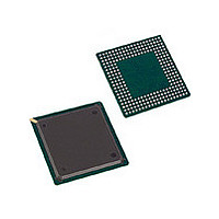
PXB4220EV3.4X Infineon Technologies, PXB4220EV3.4X Datasheet - Page 81

PXB4220EV3.4X
Manufacturer Part Number
PXB4220EV3.4X
Description
Manufacturer
Infineon Technologies
Datasheet
1.PXB4220EV3.4X.pdf
(290 pages)
Specifications of PXB4220EV3.4X
Data Rate
2.048Mbps
Number Of Channels
1
Operating Supply Voltage (typ)
3.3V
Operating Temp Range
-40C to 85C
Operating Temperature Classification
Industrial
Mounting
Surface Mount
Lead Free Status / RoHS Status
Compliant
- Current page: 81 of 290
- Download datasheet (4Mb)
4.8
4.8.1
The Upstream Loop block (UL) allows cells that are received at the Framer Interface and
forwarded to the UTOPIA Receive Interface to be send back via the UTOPIA Transmit
Interface to the Transmitter Interface. The UL block contains a buffer of 4 ATM cells.
To activate the Upstream Loop, the “p_ulp” bit in the Port Configuration Register (pcfN,
see
When a cell is available in the UL buffer, the UTOPIA transmit interface will de-assert the
TXCLAV signal, to prevent the ATM layer component from sending cells during the
processing of the loopback cell.
For ATM mode ports, all cells are looped regardless of their header. The loop is always
transparent allowing looped cells to be visible on the UTOPIA receive interface.
For AAL mode ports, it is possible to make a single channel loop using a VCI filter. When
the “vci_flt_ulp” bit in the Loopback Control Register (lpbc, see
all cells are looped. When the bit is set to 1, only those cells with the 5 LSB bits of the
VCI matching the “vci_val_ulp” field of the “lpbc” register will be looped. Loopback can
be switched from transparent to non-transparent by setting the “tulp” bit in the “lpbc”
register. If the loopback is non-transparent, looped cells are not visible on the UTOPIA
receive interface.
4.8.2
It is possible to loop ATM cells that are coming in on the UTOPIA transmit interface to
the UTOPIA receive interface through the Downstream Loop (DL) block. The DL block
contains a buffer of 4 ATM cells.
When a cell is available in the DL buffer and in the Output Queue, the UTOPIA receive
interface will transmit cells from both buffers with alternating priority.
To activate the downstream UTOPIA loop, the “p_dlp” bit in the Port Configuration
Register (pcfN, see
When the downstream UTOPIA loopback is active for at least one port, the UTOPIA
transmit interface will only assert the RxCLAV signal to 1 when a free space of one ATM
cell is available in both the DL buffer and the UT input buffer.
The loopback can be made transparent or non-transparent by setting the “tdlp” bit in the
Loopback Control Register (lpbc, see
transparent, the looped cells are not transferred to the “Cell Transmit Processing” block
CT.
Data Sheet
Chapter
Loopback Modes
Upstream Loop
Downstream Loop
7.1) must be set to 1.
Chapter
7.1) must be set to 1.
Chapter
81
PXB 4219E, PXB 4220E, PXB 4221E
7.11). If the loopback is made non-
Operational Description
Chapter
7.11) is set to 0
IWE8, V3.4
2003-01-20
Related parts for PXB4220EV3.4X
Image
Part Number
Description
Manufacturer
Datasheet
Request
R

Part Number:
Description:
IC CHIPSET 8 E1/T1 LINE 256-BGA
Manufacturer:
Infineon Technologies
Datasheet:

Part Number:
Description:
IC CHIPSET 8 E1/T1 LINE 256-BGA
Manufacturer:
Infineon Technologies
Datasheet:

Part Number:
Description:
Interworking Element for 8 E1/T1 Lines
Manufacturer:
Infineon Technologies AG
Datasheet:

Part Number:
Description:
members of Infineon ATM Chipset
Manufacturer:
Infineon Technologies AG
Datasheet:

Part Number:
Description:
Manufacturer:
Infineon Technologies AG
Datasheet:

Part Number:
Description:
Manufacturer:
Infineon Technologies AG
Datasheet:

Part Number:
Description:
Manufacturer:
Infineon Technologies AG
Datasheet:

Part Number:
Description:
Manufacturer:
Infineon Technologies AG
Datasheet:

Part Number:
Description:
Manufacturer:
Infineon Technologies AG
Datasheet:

Part Number:
Description:
Manufacturer:
Infineon Technologies AG
Datasheet:

Part Number:
Description:
Manufacturer:
Infineon Technologies AG
Datasheet:

Part Number:
Description:
16-bit microcontroller with 2x2 KByte RAM
Manufacturer:
Infineon Technologies AG
Datasheet:

Part Number:
Description:
NPN silicon RF transistor
Manufacturer:
Infineon Technologies AG
Datasheet:

Part Number:
Description:
NPN silicon RF transistor
Manufacturer:
Infineon Technologies AG
Datasheet:

Part Number:
Description:
NPN silicon RF transistor
Manufacturer:
Infineon Technologies AG
Datasheet:


