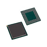
PXB4220EV3.4X Infineon Technologies, PXB4220EV3.4X Datasheet - Page 202

PXB4220EV3.4X
Manufacturer Part Number
PXB4220EV3.4X
Description
Manufacturer
Infineon Technologies
Datasheet
1.PXB4220EV3.4X.pdf
(290 pages)
Specifications of PXB4220EV3.4X
Data Rate
2.048Mbps
Number Of Channels
1
Operating Supply Voltage (typ)
3.3V
Operating Temp Range
-40C to 85C
Operating Temperature Classification
Industrial
Mounting
Surface Mount
Lead Free Status / RoHS Status
Compliant
- Current page: 202 of 290
- Download datasheet (4Mb)
7.46
Read/Write Address 00103
Reset value: 0020
gim
ds1
parc
pdcri
srst
lptd
Data Sheet
ds1
15
7
Internal
(icrcconf)
parc
Generic interface mode
0 =
1 =
DS1 Mode
0 =
1 =
Parity Check
Inverts all parity bits in the ICRC. All enabled parity checkers will
generate interrupts
0 =
1 =
Power Down Clock Recovery Interface
0 =
1 =
Software Reset
The bit srst is set by the software, but reset by the ICRC. Reading this
bit will always give the Reset value: “0”.
0 =
1 =
Loop back clock recovery interface transmitted data downstream
H
FAM: 8.192 MHz is expected/generated.
GIM: 2.048 MHz (E1) or 1.544 MHz (T1) expected/generated.
E1: The receive clocks are divided to 2.048 MHz. Output clocks
are 8.192 MHz in case of FAM or 2.048 MHz in case of GIM.
T1: The receive clocks are divided to 1.544 MHz. Output clocks
are 8.192 MHz in case of FAM or 1.544 MHz in case of GIM.
Disabled
Enabled
Normal operation
The internal clock recovery interface is put in power down mode.
No data is received, no errors are generated and the parity check
is disabled.
Normal operation
Reset ICRC
Clock
pdcri
H
Recovery
Not used
srst
202
PXB 4219E, PXB 4220E, PXB 4221E
Circuit
lptd
Configuration
lptu
Register Description
lprd
IWE8, V3.4
2003-01-20
Register
gim
lpru
8
0
Related parts for PXB4220EV3.4X
Image
Part Number
Description
Manufacturer
Datasheet
Request
R

Part Number:
Description:
IC CHIPSET 8 E1/T1 LINE 256-BGA
Manufacturer:
Infineon Technologies
Datasheet:

Part Number:
Description:
IC CHIPSET 8 E1/T1 LINE 256-BGA
Manufacturer:
Infineon Technologies
Datasheet:

Part Number:
Description:
Interworking Element for 8 E1/T1 Lines
Manufacturer:
Infineon Technologies AG
Datasheet:

Part Number:
Description:
members of Infineon ATM Chipset
Manufacturer:
Infineon Technologies AG
Datasheet:

Part Number:
Description:
Manufacturer:
Infineon Technologies AG
Datasheet:

Part Number:
Description:
Manufacturer:
Infineon Technologies AG
Datasheet:

Part Number:
Description:
Manufacturer:
Infineon Technologies AG
Datasheet:

Part Number:
Description:
Manufacturer:
Infineon Technologies AG
Datasheet:

Part Number:
Description:
Manufacturer:
Infineon Technologies AG
Datasheet:

Part Number:
Description:
Manufacturer:
Infineon Technologies AG
Datasheet:

Part Number:
Description:
Manufacturer:
Infineon Technologies AG
Datasheet:

Part Number:
Description:
16-bit microcontroller with 2x2 KByte RAM
Manufacturer:
Infineon Technologies AG
Datasheet:

Part Number:
Description:
NPN silicon RF transistor
Manufacturer:
Infineon Technologies AG
Datasheet:

Part Number:
Description:
NPN silicon RF transistor
Manufacturer:
Infineon Technologies AG
Datasheet:

Part Number:
Description:
NPN silicon RF transistor
Manufacturer:
Infineon Technologies AG
Datasheet:


