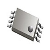
ICS853052AGT IDT, Integrated Device Technology Inc, ICS853052AGT Datasheet

ICS853052AGT
Specifications of ICS853052AGT
Related parts for ICS853052AGT
ICS853052AGT Summary of contents
Page 1
DUAL LVCMOS/LVTTL-TO-DIFFERENTIAL 2.5V, 3.3V, 5V LVPECL MULTIPLEXER G D ENERAL ESCRIPTION The ICS853052 is a Dual LVCMOS / LVTTL-to- ICS Differential 2.5V, 3.3V, 5V LVPECL Multiplexer and HiPerClockS™ a member of the HiPerClocks™ family of High Perfor mance Clocks Solutions ...
Page 2
ICS853052 DUAL LVCMOS/LVTTL-TO-DIFFERENTIAL 2.5V, 3.3V, 5V LVPECL MULTIPLEXER ABLE IN ESCRIPTIONS ...
Page 3
ICS853052 DUAL LVCMOS/LVTTL-TO-DIFFERENTIAL 2.5V, 3.3V, 5V LVPECL MULTIPLEXER BSOLUTE AXIMUM ATINGS Supply Voltage (LVPECL mode Negative Supply Voltage, V -6V (ECL mode Inputs, V (LVPECL mode) -0. Inputs, ...
Page 4
ICS853052 DUAL LVCMOS/LVTTL-TO-DIFFERENTIAL 2.5V, 3.3V, 5V LVPECL MULTIPLEXER T 4C 5V; V ABLE HARACTERISTICS ...
Page 5
ICS853052 DUAL LVCMOS/LVTTL-TO-DIFFERENTIAL 2.5V, 3.3V, 5V LVPECL MULTIPLEXER The spectral purity in a band at a specific offset from the fundamental compared to the power of the fundamental is called the dBc Phase Noise. This value is normally expressed using ...
Page 6
ICS853052 DUAL LVCMOS/LVTTL-TO-DIFFERENTIAL 2.5V, 3.3V, 5V LVPECL MULTIPLEXER P ARAMETER LVPECL V EE -3.5V to -0.375V UTPUT OAD EST IRCUIT 80% Clock 20% Outputs UTPUT ISE ...
Page 7
ICS853052 DUAL LVCMOS/LVTTL-TO-DIFFERENTIAL 2.5V, 3.3V, 5V LVPECL MULTIPLEXER ECOMMENDATIONS FOR NUSED I : NPUTS NPUTS For applications not requiring the use of a clock input, it can be left floating. Though not required, but ...
Page 8
ICS853052 DUAL LVCMOS/LVTTL-TO-DIFFERENTIAL 2.5V, 3.3V, 5V LVPECL MULTIPLEXER T 3.3V LVPECL O ERMINATION FOR The clock layout topology shown below is a typical termination for LVPECL outputs. The two different layouts mentioned are recommended only as guidelines. FOUT and nFOUT ...
Page 9
ICS853052 DUAL LVCMOS/LVTTL-TO-DIFFERENTIAL 2.5V, 3.3V, 5V LVPECL MULTIPLEXER This section provides information on power dissipation and junction temperature for the ICS853052. Equations and example calculations are also provided. 1. Power Dissipation. The total power dissipation for the ICS853052 is the ...
Page 10
ICS853052 DUAL LVCMOS/LVTTL-TO-DIFFERENTIAL 2.5V, 3.3V, 5V LVPECL MULTIPLEXER 3. Calculations and Equations. LVPECL output driver circuit and termination are shown in Figure 4. Figure 4. LVPECL Driver Circuit and Termination T o calculate worst case power dissipation into the load, ...
Page 11
ICS853052 DUAL LVCMOS/LVTTL-TO-DIFFERENTIAL 2.5V, 3.3V, 5V LVPECL MULTIPLEXER T 7A ABLE VS IR LOW ABLE FOR JA Multi-Layer PCB, JEDEC Standard Test Boards T 7B ABLE VS IR LOW ABLE FOR JA ...
Page 12
ICS853052 DUAL LVCMOS/LVTTL-TO-DIFFERENTIAL 2.5V, 3.3V, 5V LVPECL MULTIPLEXER ACKAGE UTLINE UFFIX FOR T 8A ABLE ACKAGE IMENSIONS ...
Page 13
ICS853052 DUAL LVCMOS/LVTTL-TO-DIFFERENTIAL 2.5V, 3.3V, 5V LVPECL MULTIPLEXER ABLE RDERING NFORMATION ...
Page 14
ICS853052 DUAL LVCMOS/LVTTL-TO-DIFFERENTIAL 2.5V, 3.3V, 5V LVPECL MULTIPLEXER Innovate with IDT and accelerate your future networks. Contact: www.IDT.com For Sales 800-345-7015 408-284-8200 Fax: 408-284-2775 Corporate Headquarters Integrated Device Technology, Inc. 6024 Silver Creek Valley Road San Jose, CA 95138 United ...


