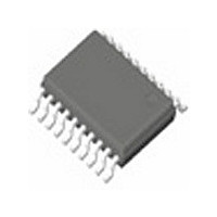
ICS85314BGI-01T IDT, Integrated Device Technology Inc, ICS85314BGI-01T Datasheet - Page 11

ICS85314BGI-01T
Manufacturer Part Number
ICS85314BGI-01T
Description
Manufacturer
IDT, Integrated Device Technology Inc
Type
Clock Driverr
Datasheet
1.ICS85314BGI-01T.pdf
(20 pages)
Specifications of ICS85314BGI-01T
Number Of Clock Inputs
2
Output Frequency
700MHz
Output Logic Level
LVPECL
Operating Supply Voltage (min)
2.375V
Operating Supply Voltage (typ)
3.3V
Operating Supply Voltage (max)
3.8V
Package Type
TSSOP
Operating Temp Range
-40C to 85C
Operating Temperature Classification
Industrial
Mounting
Surface Mount
Pin Count
20
Lead Free Status / RoHS Status
Not Compliant
T
85314BGI-01
The clock layout topology shown below is a typical termina-
tion for LVPECL outputs. The two different layouts mentioned
are recommended only as guidelines.
FOUT and nFOUT are low impedance follower outputs that gen-
erate ECL/LVPECL compatible outputs. Therefore, terminating
resistors (DC current path to ground) or current sources must
be used for functionality. These outputs are designed to drive
RTT =
ERMINATION FOR
((V
FOUT
F
OH
IGURE
+ V
OL
4A. LVPECL O
) / (V
1
3.3V LVPECL O
CC
Z
Z
– 2)) – 2
o
o
= 50
= 50
Z
o
50
UTPUT
T
RTT
ERMINATION
UTPUTS
50
V
D
CC
FIN
- 2V
IFFERENTIAL
www.idt.com
11
50 transmission lines. Matched impedance techniques should
be used to maximize operating frequency and minimize signal
distortion. Figures 4A and 4B show two different layouts which
are recommended only as guidelines. Other suitable clock lay-
outs may exist and it would be recommended that the board
designers simulate to guarantee compatibility across all printed
circuit and clock component process variations.
-
TO
-2.5V/3.3V LVPECL F
FOUT
F
IGURE
4B. LVPECL O
Z
Z
o
o
= 50
= 50
125
84
ICS85314I-01
UTPUT
L
OW
3.3V
T
125
84
ANOUT
ERMINATION
S
KEW
REV. F JULY 25, 2010
FIN
, 1-
B
UFFER
TO
-5


