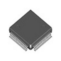
IDT5T93GL161PFI IDT, Integrated Device Technology Inc, IDT5T93GL161PFI Datasheet - Page 8

IDT5T93GL161PFI
Manufacturer Part Number
IDT5T93GL161PFI
Description
Manufacturer
IDT, Integrated Device Technology Inc
Type
Clock Driverr
Datasheet
1.IDT5T93GL161PFI.pdf
(20 pages)
Specifications of IDT5T93GL161PFI
Number Of Clock Inputs
2
Mode Of Operation
Differential
Output Frequency
450MHz
Output Logic Level
LVDS
Operating Supply Voltage (min)
2.3V
Operating Supply Voltage (typ)
2.5V
Operating Supply Voltage (max)
2.7V
Package Type
TQFP
Operating Temp Range
-40C to 85C
Operating Temperature Classification
Industrial
Mounting
Surface Mount
Pin Count
64
Quiescent Current
350mA
Lead Free Status / RoHS Status
Not Compliant
Table 5B. eHSTL AC Differential Input Characteristics, T
NOTE 1.The 1V peak-to-peak input pulse level is specified to allow consistent, repeatable results in an automatic test equipment (ATE)
environment. This device meets the V
NOTE 2.A 900mV crossing point level is specified to allow consistent, repeatable results in an automatic test equipment (ATE)
environment. This device meets the V
NOTE 3.In all cases, input waveform timing is marked at the differential cross-point of the input signals.
NOTE 4.The input signal edge rate of 2V/ns or greater is to be maintained in the 20% to 80% range of the input waveform.
Table 5C. LVEPECL (2.5V) and LVPECL (3.3V) Differential Input AC Characteristics, T
NOTE 1.The 732mV peak-to-peak input pulse level is specified to allow consistent, repeatable results in an automatic test equipment
(ATE) environment. This device meets the V
NOTE 2.A 1082mV LVEPECL (2.5V) and 1880mV LVPECL (3.3V) crossing point level is specified to allow consistent, repeatable results
in an automatic test equipment (ATE) environment. This device meets the V
NOTE 3.In all cases, input waveform timing is marked at the differential cross-point of the input signals.
N
Table 5D. LVDS Differential Input AC Characteristics, T
NOTE 1.The 400mV peak-to-peak input pulse level is specified to allow consistent, repeatable results in an automatic test equipment
(ATE) environment. This device meets the V
NOTE 2.A 1.2V crossing point level is specified to allow consistent, repeatable results in an automatic test equipment (ATE) environment.
This device meets the V
NOTE 3.In all cases, input waveform timing is marked at the differential cross-point of the input signals.
N
IDT™ LVDS GLITCHLESS CLOCK BUFFER TERABUFFER™ II
Symbol
V
V
D
V
t
Symbol
V
V
D
V
t
Symbol
V
V
D
V
t
OTE 4.The input signal edge rate of 2V/ns or greater is to be maintained in the 20% to 80% range of the input waveform.
OTE 4.The input signal edge rate of 2V/ns or greater is to be maintained in the 20% to 80% range of the input waveform.
R
R
R
IDT5T93GL161
2.5V LVDS 1:16 GLITCHLESS CLOCK BUFFER TERABUFFER™ II
DIF
X
THI
DIF
X
THI
DIF
X
THI
H
H
H
/ t
/ t
/ t
F
F
F
Parameter
Input Signal Swing
Differential Input Signal Crossing Point
Duty Cycle
Input Timing Measurement Reference Level
Input Signal Edge Rate
Parameter
Input Signal Swing
Differential Input Cross Point Voltage
Duty Cycle
Input Timing Measurement Reference Level
Input Signal Edge Rate
Parameter
Input Signal Swing
Differential Input Cross Point Voltage
Duty Cycle
Input Timing Measurement Reference Level
Input Signal Edge Rate
X
specification under actual use conditions.
(1)
(1)
(1)
(4)
(4)
(4)
DIF
X
specification under actual use conditions.
(AC) specification under actual use conditions.
DIF
DIF
(AC) specification under actual use conditions.
(AC) specification under actual use conditions.
(2)
(2)
(2)
(3)
(3)
(3)
A
A
= -40°C to 85°C
8
= -40°C to 85°C
LVEPECL
LVPECL
X
specification under actual use conditions.
IDT5T93GL161 REV. A SEPTEMBER 12, 2008
A
= -40°C to 85°C
Crossing Point
Crossing Point
Crossing Point
Maximum
Maximum
Value
1082
1880
900
732
50
50
1
2
2
400
1.2
50
2
Units
Units
Units
V/ns
V/ns
V/ns
mV
mV
mV
mV
m
%
%
%
V
V
V
V
V


