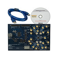
AD9959/PCB Analog Devices Inc, AD9959/PCB Datasheet - Page 4
AD9959/PCB
Manufacturer Part Number
AD9959/PCB
Description
Manufacturer
Analog Devices Inc
Datasheet
1.AD9959PCB.pdf
(28 pages)
Specifications of AD9959/PCB
Lead Free Status / RoHS Status
Not Compliant


AD9959/PCB
Manual I/O Control Headers
Provides the interface for communication with the AD9959
when the part is under the control of an external controller
(manual control). See Eval Board Control for correct jumper
settings.
Multi Device Synchronous Control
These connections set up the AD9959 for multi device
synchronous operation.
DAC Channels
These connections represent the DAC filtered/unfiltered output
and AVDD power supply.
Clock Input Supply
Powers the AD9959’s clock input circuitry.
Clock Mode Select
Controls whether the part is driven by a 20 MHz to 30 MHz
crystal provided by the user, or by an external signal generator,
such as Ref Clk.
Ref Clk Input
Input for the external Ref Clk signal.
EVALUATION
CONTROL
BOARD
PORT
USB
SDIO
MANUAL I/O
CONTROL
HEADERS
EVALUATION BOARD LAYOUT
RU/RD
CONTROL
Rev. 0 | Page 4 of 28
MULTI DEVICE
SYNCHRONOUS
CONTROL
Figure 2.
POWER
SUPPLY
Band Gap Supply
Provides the voltage needed for band gap functionality.
Power Supply
Powers the AD9959’s USB circuitry, I/O circuitry, and the
digital portion (DVDD) of the DACs. Note AVDD is not
powered via this connector (TB1).
RU/RD Control, SDIO
Jumpers W6, W5, and W4 must be set to control the Ramp
Up/Ramp Down feature using the SDIO pins.
USB Port
When the part is under PC control (default mode), the evaluation
board communicates with the AD9959 via this port.
Eval Board Control
These jumpers set up the AD9959 for manual or PC control
(control through the USB port). Figure 3 shows the correct
jumper placements for PC control. For manual control remove
jumpers W0, W1, W2, and W3; set W7 on the manual control
pin (move jumper one position to the left).
DAC
CHANNEL 1
DAC
CHANNEL 2
DAC
CHANNEL 0
DAC
CHANNEL 3
CLOCK
INPUT
SUPPLY
BAND
GAP
SUPPLY
CLOCK
MODE
SELECT
REF CLK
INPUT