AD9959/PCB Analog Devices Inc, AD9959/PCB Datasheet - Page 19
AD9959/PCB
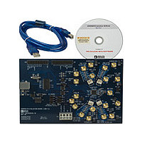
Manufacturer Part Number
AD9959/PCB
Description
Manufacturer
Analog Devices Inc
Datasheet
1.AD9959PCB.pdf
(28 pages)
Specifications of AD9959/PCB
Lead Free Status / RoHS Status
Not Compliant


In the Channel Output Config window (Figure 39), Channel 0 has a frequency output of 10 MHz (Frequency 00 box), Channel 1 an
output frequency of 20 MHz, Channel 2 an output frequency of 30 MHz, and Channel 3 has a frequency output of 40 MHz. Because the
RU/RD operation is enabled, the Enable ASF and Enable Auto ASF boxes are checked. The amplitude scalar factor (ASF) is set to 1 (full
scale). Therefore, the output signal will be 0 MHz until the correct profile pin is selected to ramp the frequency up to full scale. When this
setup file is loaded, profile pins P0, P1, P2, and P3 are pressed as shown in the Profile and RURD Pin Control Section. P0 controls
Channel 0, P1 controls Channel 1, P2 controls Channel 2, and P3 controls Channel 3. If a profile pin is deselected, the associated
channel’s output will return to 0 MHz. To return to full scale, re-press the profile pin that triggers the RU/RD operation.
Modulation Mode
Open the Modulation Mode folder to access the modulation mode of operation example setup files. Once this folder is opened you will
be presented with the window shown in Figure 40.
For frequency modulation (FSK), open the Frequency folder; for phase modulation (PSK), open the Phase folder; and for amplitude
modulation (ASK), open the Amplitude folder. In these folders, all setup files are indexed by their level (2, 4, 8, or 16-level). This section
discusses the CH2_@3 MHz increments.stp file found in the Frequency folder under the 16-level folder.
Rev. 0 | Page 19 of 28
Figure 39.
Figure 40.
AD9959/PCB