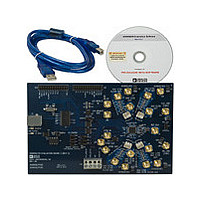
AD9959/PCB Analog Devices Inc, AD9959/PCB Datasheet - Page 10
AD9959/PCB
Manufacturer Part Number
AD9959/PCB
Description
Manufacturer
Analog Devices Inc
Datasheet
1.AD9959PCB.pdf
(28 pages)
Specifications of AD9959/PCB
Lead Free Status / RoHS Status
Not Compliant


AD9959/PCB
CP Current selects the charge pump current output of the
PLL in the Ref Clock Multiplier circuitry. Selecting a higher
current output will result in the loop locking faster, but there
is a trade-off. Increasing this current output will also increase
phase noise. The default setting of this box is 75 μA.
System Clock displays the operating frequency the DDS core
(system). The value shown here is derived from the values
entered in the Ref Clock and Multiplier boxes.
VCO Gain is automatically set when the Ref Clock Multiplier is
being used to generate a system clock that is greater than
255 MHz. This is done to ensure stability of the Ref Clock
Multiplier circuitry. A pop-up window will appear alerting you
to this update (see Figure 20).
Please refer to the Reference Clock Modes section of the
AD9959 data sheet for more information regarding clock
modes and operation.
3. All Channel Accumulator Control
The All Channel Accumulator Control provides control over
the phase and sweep accumulators for all channels.
Check the Auto Clear Phase Accumulator or Auto Clear
Sweep Accumulator boxes to clear and release the
corresponding accumulator. The auto clear function sets the
accumulator to 0 and then begins accumulating.
Select the Clear Phase Accumulator or Clear Sweep
Accumulator to clear and hold the corresponding accumulator.
The clear function clears and then holds the contents of the
corresponding accumulator to 0 until the box is unchecked.
4. Modulation Configuration
The Modulation Configuration section configures the
modulation operation of the AD9959.
Profile Pin Configuration provides access to the PPC Bits
(FR1<14:12>). These bits are used to control the modulation
scheme of the AD9959. PPC Bit 0 is the LSB (FR1<12>), and
PPC Bit 2 is the MSB (FR1<14>).When a PPC bit is selected, it
is set to Logic 1 from its default setting of 0. These bits are
discussed in more detail in the Modulation Mode section of the
data sheet.
RU/RD assigns which pins will control the scaling (Ramp
Up/Ramp Down) of the output amplitude of the AD9959. This
feature can be controlled via the profile or SDIO data pins.
Figure 20.
Rev. 0 | Page 10 of 28
Select Use Profile Pins 2 & 3 if you would like to control the
RU/RD feature with Profile Pin 2 and Profile Pin 3, or Use
Profile Pin 3 to control this feature using only Profile Pin 3. If
you wish to use the SDIO data pins to control this feature,
simply select Use SDIO pins 1, 2, & 3. Note that to use the
SDIO pins to control the RU/RD feature, the SDIO RU/RD
Control jumpers must be placed (see Figure 2). The default
setting of this box is RU/RD Disabled. In this mode, you will
not be able scale the output amplitude.
The AD9959 can be configured to perform many operations in
various combinations. Please refer to the Channel Constraint
Guidelines and the Modulation Mode sections of the AD9959
data sheet for more details regarding the use of the RU/RD
function in combination with the different modes of operation
(single-tone, modulation, linear sweep) of the AD9959. For
more information regarding the theory of the RU/RD
operation, note the Output Amplitude Control Mode section of
the AD9959 data sheet.
Level selects the desired level of modulation of the AD9959.
The AD9959 can perform 2-level, 4-level, 8-level, or 16-level
modulation of frequency, phase, or amplitude (FSK, PSK, ASK).
This modulation is controlled via the data pins; note the
Channel Constraint Guidelines and the Modulation Mode
sections of the AD9959 data sheet for more details.
5. Multi Device Sync
It is possible to synchronize multiple evaluation boards. Refer to
the Synchronizing Multiple AD9959 Devices section in the
AD9959 data sheet and the evaluation board schematic (located
in the schematic folder of the AD9958_59 evaluation software
CD) for more details on synchronizing multiple AD9959s.
6. All Channel Power Down
The All Channel Power Down section allows you to power
down all channels collectively using software configurations or
the external power down options found in the External PD
Control subsection.
Select the Clock Input, DAC Ref, or Disable SyncCLK Out
boxes to power down those circuit blocks respectively for each
individual channel. Once the selection has been made, click the
LOAD button to execute the power down.
When using the External PD Control, select from the Power
Down Pin Mode: Quick Recovery (default setting) or Full
Power Down mode. In quick recovery mode, only the digital
logic is powered down whereas all functions are powered down
in full power down mode. To execute the power down when
using external PD control, you must click the Power Down Pin.
When pressed, the power down pin is at Logic 1, indicating
the powered down mode. When this pin is not pressed, it is at
Logic 0, indicating the powered up mode.