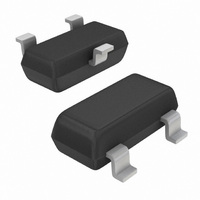
BCW72LT1G ON Semiconductor, BCW72LT1G Datasheet - Page 6

BCW72LT1G
Manufacturer Part Number
BCW72LT1G
Description
TRANS NPN GP 45V 100MA SOT-23
Manufacturer
ON Semiconductor
Datasheet
1.BCW72LT1G.pdf
(7 pages)
Specifications of BCW72LT1G
Transistor Type
NPN
Current - Collector (ic) (max)
100mA
Voltage - Collector Emitter Breakdown (max)
45V
Vce Saturation (max) @ Ib, Ic
210mV @ 2.5mA, 50mA
Dc Current Gain (hfe) (min) @ Ic, Vce
200 @ 2mA, 5V
Power - Max
225mW
Frequency - Transition
300MHz
Mounting Type
Surface Mount
Package / Case
SOT-23-3, TO-236-3, Micro3™, SSD3, SST3
Configuration
Single
Transistor Polarity
NPN
Mounting Style
SMD/SMT
Collector- Emitter Voltage Vceo Max
45 V
Emitter- Base Voltage Vebo
5 V
Continuous Collector Current
0.1 A
Maximum Dc Collector Current
0.1 A
Power Dissipation
225 mW
Maximum Operating Frequency
300 MHz
Maximum Operating Temperature
+ 150 C
Dc Collector/base Gain Hfe Min
200 at 2 mA at 5 V
Minimum Operating Temperature
- 55 C
Number Of Elements
1
Collector-emitter Voltage
45V
Collector-base Voltage
50V
Emitter-base Voltage
5V
Collector Current (dc) (max)
100mA
Dc Current Gain (min)
200
Frequency (max)
300MHz
Operating Temp Range
-55C to 150C
Operating Temperature Classification
Military
Mounting
Surface Mount
Pin Count
3
Package Type
SOT-23
Lead Free Status / RoHS Status
Lead free / RoHS Compliant
Current - Collector Cutoff (max)
-
Lead Free Status / Rohs Status
Lead free / RoHS Compliant
Available stocks
Company
Part Number
Manufacturer
Quantity
Price
Company:
Part Number:
BCW72LT1G
Manufacturer:
ON
Quantity:
30 000
Company:
Part Number:
BCW72LT1G
Manufacturer:
STACKPOLE
Quantity:
4 856
10
10
400
200
100
10
10
10
10
10
4.0
6.0
60
20
10
40
-1
-2
0.07
0.05
0.03
0.02
0.01
4
1
0
3
2
1.0
0.7
0.5
0.3
0.2
0.1
2.0
- 4
0
0.01
V
CC
- 2
0
0.02
= 30 Vdc
V
D = 0.5
0.01
CE
0
0.05
0.02
, COLLECTOR-EMITTER VOLTAGE (VOLTS)
4.0
0.2
0.1
0.05
T
T
CURRENT LIMIT
THERMAL LIMIT
SECOND BREAKDOWN LIMIT
J
J
, JUNCTION TEMPERATURE (°C)
+ 20 + 40 + 60 + 80 + 100 + 120 + 140 + 160
= 150°C
0.1
6.0
T
Figure 19A.
A
Figure 20.
= 25°C
0.2
8.0 10
T
SINGLE PULSE
C
I
= 25°C
CEO
0.5
I
dc
CEX
1.0 ms
1.0
@ V
dc
100 ms
BE(off)
10 ms
2.0
I
AND
CBO
20
1.0 s
= 3.0 Vdc
Figure 19. Thermal Response
5.0
http://onsemi.com
10
40
t, TIME (ms)
6
20
as shown in Figure 19A. Using the model and the device thermal
response the normalized effective transient thermal resistance of
Figure 19 was calculated for various duty cycles.
steady state value R
Example:
The MPS3904 is dissipating 2.0 watts peak under the following
conditions:
Using Figure 19 at a pulse width of 1.0 ms and D = 0.2, the reading of
r(t) is 0.22.
The peak rise in junction temperature is therefore
For more information, see AN−569.
transistor that must be observed for reliable operation. Collector load
lines for specific circuits must fall below the limits indicated by the
applicable curve.
variable depending upon conditions. Pulse curves are valid for duty
cycles to 10% provided T
the data in Figure 19. At high case or ambient temperatures, thermal
limitations will reduce the power that can be handled to values less
than the limitations imposed by second breakdown.
DESIGN NOTE: USE OF THERMAL RESPONSE DATA
A train of periodical power pulses can be represented by the model
To find Z
t
DT = r(t) x P
The safe operating area curves indicate I
The data of Figure 20 is based upon T
1
= 1.0 ms, t
50
qJA(t)
100 200
P
(pk)
(pk)
2
, multiply the value obtained from Figure 19 by the
= 5.0 ms. (D = 0.2)
x R
qJA
qJA
FIGURE 19A
t
1
.
500 1.0 k 2.0 k
J(pk)
t
= 0.22 x 2.0 x 200 = 88°C.
2
≤ 150°C. T
DUTY CYCLE, D = t
D CURVES APPLY FOR POWER
PULSE TRAIN SHOWN
READ TIME AT t
Z
T
qJA(t)
J(pk)
J(pk)
− T
J(pk)
= r(t) • R
5.0 k 10 k 20 k
A
may be calculated from
= P
= 150°C; T
C
−V
(pk)
qJA
1
CE
Z
(SEE AN−569)
qJA(t)
1
/t
limits of the
2
C
or T
50 k 1 00 k
A
is


