MMBT4401LT3G ON Semiconductor, MMBT4401LT3G Datasheet - Page 2
MMBT4401LT3G
Manufacturer Part Number
MMBT4401LT3G
Description
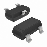
TRANS NPN GP 40V 600MA SOT-23
Manufacturer
ON Semiconductor
Datasheet
1.MMBT4401LT3G.pdf
(7 pages)
Specifications of MMBT4401LT3G
Transistor Type
NPN
Current - Collector (ic) (max)
600mA
Voltage - Collector Emitter Breakdown (max)
40V
Vce Saturation (max) @ Ib, Ic
750mV @ 50mA, 500mA
Dc Current Gain (hfe) (min) @ Ic, Vce
100 @ 150mA, 1V
Power - Max
225mW
Frequency - Transition
250MHz
Mounting Type
Surface Mount
Package / Case
SOT-23-3, TO-236-3, Micro3™, SSD3, SST3
Transistor Polarity
NPN
Number Of Elements
1
Collector-emitter Voltage
40V
Collector-base Voltage
60V
Emitter-base Voltage
6V
Collector Current (dc) (max)
600mA
Power Dissipation
300mW
Frequency (max)
250MHz
Operating Temp Range
-55C to 150C
Operating Temperature Classification
Military
Mounting
Surface Mount
Pin Count
3
Package Type
SOT-23
Lead Free Status / RoHS Status
Lead free / RoHS Compliant
Current - Collector Cutoff (max)
-
Lead Free Status / Rohs Status
Compliant
Available stocks
Company
Part Number
Manufacturer
Quantity
Price
Company:

Part Number:
MMBT4401LT3G
Manufacturer:
ON Semiconductor
Quantity:
40 000
Company:
Part Number:
MMBT4401LT3G
Manufacturer:
ON
Quantity:
30 000
Company:
Part Number:
MMBT4401LT3G
Manufacturer:
TE
Quantity:
2 527
Part Number:
MMBT4401LT3G
Manufacturer:
ON/安森美
Quantity:
20 000


3. Pulse Test: Pulse Width ≤ 300 ms, Duty Cycle ≤ 2.0%.
ELECTRICAL CHARACTERISTICS
OFF CHARACTERISTICS
ON CHARACTERISTICS (Note 3)
SMALL−SIGNAL CHARACTERISTICS
SWITCHING CHARACTERISTICS
Collector −Emitter Breakdown Voltage (Note 3)
Collector −Base Breakdown Voltage
Emitter −Base Breakdown Voltage
Base Cutoff Current
Collector Cutoff Current
DC Current Gain
Collector −Emitter Saturation Voltage
Base −Emitter Saturation Voltage
Current −Gain − Bandwidth Product
Collector−Base Capacitance
Emitter−Base Capacitance
Input Impedance
Voltage Feedback Ratio
Small −Signal Current Gain
Output Admittance
Delay Time
Rise Time
Storage Time
Fall Time
- 2.0 V
+16 V
0
< 2.0 ns
Figure 1. Turn−On Time
1.0 to 100 ms,
DUTY CYCLE ≈ 2.0%
1.0 kW
Characteristic
SWITCHING TIME EQUIVALENT TEST CIRCUITS
(I
(I
(I
(I
(I
C
C
C
C
C
(T
= 20 mAdc, V
= 1.0 mAdc, V
= 1.0 mAdc, V
= 1.0 mAdc, V
= 1.0 mAdc, V
A
= 25°C unless otherwise noted)
(V
(V
I
(V
(V
+ 30 V
200 W
C
CB
EB
Scope rise time < 4.0 ns
*Total shunt capacitance of test jig connectors, and oscilloscope
CC
(I
(I
CC
= 150 mAdc, I
(I
(I
(I
(I
(I
(I
(V
(V
(I
C
C
= 5.0 Vdc, I
= 0.5 Vdc, I
C
C
C
C
C
C
C
I
= 30 Vdc, I
C
= 30 Vdc, V
CE
CE
= 150 mAdc, V
= 500 mAdc, V
B1
= 0.1 mAdc, V
= 1.0 mAdc, V
= 150 mAdc, I
= 500 mAdc, I
= 150 mAdc, I
= 500 mAdc, I
S
= 10 mAdc, V
CE
* < 10 pF
= I
http://onsemi.com
= 35 Vdc, V
= 35 Vdc, V
CE
CE
CE
CE
= 10 Vdc, f = 100 MHz)
B2
(I
(I
(I
= 10 Vdc, f = 1.0 kHz)
= 10 Vdc, f = 1.0 kHz)
= 10 Vdc, f = 1.0 kHz)
= 10 Vdc, f = 1.0 kHz)
C
C
E
= 15 mAdc)
= 0.1 mAdc, I
= 1.0 mAdc, I
= 0.1 mAdc, I
C
E
C
B1
= 0, f = 1.0 MHz)
= 0, f = 1.0 MHz)
EB
= 150 mAdc,
2
= 15 mAdc)
CE
CE
CE
CE
CE
= 2.0 Vdc,
EB
EB
B
B
B
B
= 15 mAdc)
= 50 mAdc)
= 15 mAdc)
= 50 mAdc)
= 0.4 Vdc)
= 0.4 Vdc)
= 1.0 Vdc)
= 1.0 Vdc)
= 1.0 Vdc)
= 1.0 Vdc)
= 2.0 Vdc)
+16 V
0
B
E
C
-14 V
= 0)
= 0)
= 0)
V
V
V
Figure 2. Turn−Off Time
Symbol
V
V
1.0 to 100 ms,
DUTY CYCLE ≈ 2.0%
(BR)CEO
(BR)CBO
(BR)EBO
I
CE(sat)
BE(sat)
I
h
C
C
BEV
CEX
h
h
h
< 20 ns
h
f
t
t
FE
t
t
oe
T
eb
cb
ie
re
fe
d
s
r
f
1.0 kW
0.75
Min
100
250
6.0
1.0
0.1
1.0
40
60
20
40
80
40
40
−
−
−
−
−
−
−
−
−
−
−
- 4.0 V
Max
0.75
0.95
300
500
225
0.1
0.1
0.4
1.2
6.5
8.0
30
15
30
15
20
30
−
−
−
−
−
−
−
−
+ 30 V
200 W
C
S
* < 10 pF
X 10
mmhos
mAdc
mAdc
MHz
Unit
Vdc
Vdc
Vdc
Vdc
Vdc
pF
pF
kW
ns
ns
−
−
− 4
Related parts for MMBT4401LT3G
Image
Part Number
Description
Manufacturer
Datasheet
Request
R

Part Number:
Description:
ON Semiconductor [VOLTAGE REGULATOR]
Manufacturer:
ON Semiconductor
Datasheet:
Part Number:
Description:
357-036-542-201 CARDEDGE 36POS DL .156 BLK LOPRO
Manufacturer:
ON Semiconductor
Datasheet:
Part Number:
Description:
357-036-542-201 CARDEDGE 36POS DL .156 BLK LOPRO
Manufacturer:
ON Semiconductor
Datasheet:
Part Number:
Description:
357-036-542-201 CARDEDGE 36POS DL .156 BLK LOPRO
Manufacturer:
ON Semiconductor
Datasheet:
Part Number:
Description:
357-036-542-201 CARDEDGE 36POS DL .156 BLK LOPRO
Manufacturer:
ON Semiconductor
Datasheet:
Part Number:
Description:
357-036-542-201 CARDEDGE 36POS DL .156 BLK LOPRO
Manufacturer:
ON Semiconductor
Datasheet:
Part Number:
Description:
357-036-542-201 CARDEDGE 36POS DL .156 BLK LOPRO
Manufacturer:
ON Semiconductor
Datasheet:
Part Number:
Description:
357-036-542-201 CARDEDGE 36POS DL .156 BLK LOPRO
Manufacturer:
ON Semiconductor
Datasheet:
Part Number:
Description:
357-036-542-201 CARDEDGE 36POS DL .156 BLK LOPRO
Manufacturer:
ON Semiconductor
Datasheet:
Part Number:
Description:
357-036-542-201 CARDEDGE 36POS DL .156 BLK LOPRO
Manufacturer:
ON Semiconductor
Datasheet:
Part Number:
Description:
357-036-542-201 CARDEDGE 36POS DL .156 BLK LOPRO
Manufacturer:
ON Semiconductor
Datasheet:
Part Number:
Description:
Manufacturer:
ON Semiconductor
Datasheet:
Part Number:
Description:
Manufacturer:
ON Semiconductor
Datasheet:
Part Number:
Description:
Manufacturer:
ON Semiconductor
Datasheet: