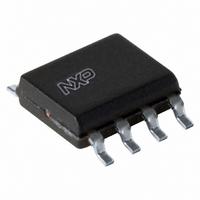
PBLS2002S,115 NXP Semiconductors, PBLS2002S,115 Datasheet - Page 7

PBLS2002S,115
Manufacturer Part Number
PBLS2002S,115
Description
LOADSWITCH PNP 20V 3A 8-SOIC
Manufacturer
NXP Semiconductors
Series
-r
Datasheet
1.PBLS2002S115.pdf
(16 pages)
Specifications of PBLS2002S,115
Package / Case
8-SOIC (3.9mm Width)
Transistor Type
1 NPN Pre-Biased, 1 PNP
Current - Collector (ic) (max)
100mA, 3A
Voltage - Collector Emitter Breakdown (max)
50V, 20V
Resistor - Base (r1) (ohms)
4.7K
Resistor - Emitter Base (r2) (ohms)
4.7K
Dc Current Gain (hfe) (min) @ Ic, Vce
30 @ 10mA, 5V / 150 @ 2A, 2V
Vce Saturation (max) @ Ib, Ic
150mV @ 500µA, 10mA / 355mV @ 300mA, 3A
Current - Collector Cutoff (max)
1µA, 100nA
Frequency - Transition
100MHz
Power - Max
1.5W
Mounting Type
Surface Mount
Configuration
Dual Dual Collector
Transistor Polarity
NPN/PNP
Typical Input Resistor
4.7 KOhms at NPN
Typical Resistor Ratio
1 at NPN
Mounting Style
SMD/SMT
Collector- Emitter Voltage Vceo Max
50 V at NPN, 20 V at PNP
Peak Dc Collector Current
100 mA at NPN, 3000 mA at PNP
Maximum Operating Temperature
+ 150 C
Minimum Operating Temperature
- 65 C
Lead Free Status / RoHS Status
Lead free / RoHS Compliant
Lead Free Status / RoHS Status
Lead free / RoHS Compliant, Lead free / RoHS Compliant
Other names
934060278115
PBLS2002S T/R
PBLS2002S T/R
PBLS2002S T/R
PBLS2002S T/R
NXP Semiconductors
PBLS2002S_2
Product data sheet
Table 7.
T
[1]
Symbol
V
V
t
t
t
t
t
t
f
C
TR2; NPN resistor-equipped transistor
I
I
I
h
V
V
V
R1
R2/R1
C
d
r
on
s
f
off
T
CBO
CEO
EBO
amb
FE
BEsat
BEon
CEsat
I(off)
I(on)
c
c
Pulse test: t
= 25 C unless otherwise specified
Parameter
base-emitter
saturation voltage
base-emitter turn-on
voltage
delay time
rise time
turn-on time
storage time
fall time
turn-off time
transition frequency
collector capacitance
collector-base cut-off
current
collector-emitter
cut-off current
emitter-base cut-off
current
DC current gain
collector-emitter
saturation voltage
off-state input voltage V
on-state input voltage V
bias resistor 1 (input)
bias resistor ratio
collector capacitance
Characteristics
p
300 s;
Rev. 02 — 24 August 2009
0.02
…continued
Conditions
I
I
V
I
I
I
f = 100 MHz
V
f = 1 MHz
V
V
V
T
V
V
I
V
f = 1 MHz
C
C
C
Boff
C
C
j
CE
CB
CB
CE
CE
EB
CE
CE
CE
CB
= 150 C
= 2 A; I
= 3 A; I
= 2 A; I
= 100 mA; V
= 10 mA; I
= 100 mA
= 5 V; I
= 2 V; I
= 10 V; I
= 50 V; I
= 30 V; I
= 30 V; I
= 5 V; I
= 5 V; I
= 0.3 V; I
= 10 V; I
B
B
Bon
C
C
C
= 100 mA
= 300 mA
C
E
B
B
B
E
= 0 A
= 10 mA
= 100 A
C
E
= 100 mA;
= 0.5 mA
= 1 A
= 0 A
= 0 A
= 0 A;
= i
= 20 mA
= i
CE
e
e
= 0 A;
= 5 V;
= 0 A;
[1]
[1]
[1]
20 V PNP BISS loadswitch
Min
-
-
-
-
-
-
-
-
-
100
-
-
-
-
-
30
-
-
2.5
3.3
0.8
-
PBLS2002S
Typ
7
34
41
175
30
205
-
-
-
-
-
-
-
-
1.1
1.9
4.7
1
-
0.95
1
0.8
© NXP B.V. 2009. All rights reserved.
Max
-
-
-
-
-
-
-
50
100
1
50
900
-
150
0.5
-
6.1
1.2
2.5
1.1
1.2
1.2
Unit
V
V
V
ns
ns
ns
ns
ns
ns
MHz
pF
nA
mV
V
V
k
pF
7 of 16
A
A
A


