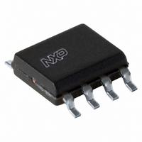
PBLS2002S,115 NXP Semiconductors, PBLS2002S,115 Datasheet - Page 11

PBLS2002S,115
Manufacturer Part Number
PBLS2002S,115
Description
LOADSWITCH PNP 20V 3A 8-SOIC
Manufacturer
NXP Semiconductors
Series
-r
Datasheet
1.PBLS2002S115.pdf
(16 pages)
Specifications of PBLS2002S,115
Package / Case
8-SOIC (3.9mm Width)
Transistor Type
1 NPN Pre-Biased, 1 PNP
Current - Collector (ic) (max)
100mA, 3A
Voltage - Collector Emitter Breakdown (max)
50V, 20V
Resistor - Base (r1) (ohms)
4.7K
Resistor - Emitter Base (r2) (ohms)
4.7K
Dc Current Gain (hfe) (min) @ Ic, Vce
30 @ 10mA, 5V / 150 @ 2A, 2V
Vce Saturation (max) @ Ib, Ic
150mV @ 500µA, 10mA / 355mV @ 300mA, 3A
Current - Collector Cutoff (max)
1µA, 100nA
Frequency - Transition
100MHz
Power - Max
1.5W
Mounting Type
Surface Mount
Configuration
Dual Dual Collector
Transistor Polarity
NPN/PNP
Typical Input Resistor
4.7 KOhms at NPN
Typical Resistor Ratio
1 at NPN
Mounting Style
SMD/SMT
Collector- Emitter Voltage Vceo Max
50 V at NPN, 20 V at PNP
Peak Dc Collector Current
100 mA at NPN, 3000 mA at PNP
Maximum Operating Temperature
+ 150 C
Minimum Operating Temperature
- 65 C
Lead Free Status / RoHS Status
Lead free / RoHS Compliant
Lead Free Status / RoHS Status
Lead free / RoHS Compliant, Lead free / RoHS Compliant
Other names
934060278115
PBLS2002S T/R
PBLS2002S T/R
PBLS2002S T/R
PBLS2002S T/R
NXP Semiconductors
8. Test information
PBLS2002S_2
Product data sheet
Fig 17. BISS transistor switching time definition
Fig 18. Test circuit for switching times
90 %
10 %
90 %
10 %
I
I
B
C
I
C
= 2 A; I
oscilloscope
t
d
Bon
t
on
= 100 mA; I
Rev. 02 — 24 August 2009
V
t
I
r
(probe)
450
Boff
R1
= 100 mA; R1 = open; R2 = 25 ; R
R2
R
B
V
BB
R
C
V
CC
DUT
V
o
mgd624
(probe)
I
450
Bon
t
s
I
(100 %)
Boff
t
20 V PNP BISS loadswitch
off
B
oscilloscope
PBLS2002S
= 70 ; R
input pulse
(idealized waveform)
output pulse
(idealized waveform)
© NXP B.V. 2009. All rights reserved.
t
C
f
= 5
I
006aaa266
C
(100 %)
11 of 16
t


