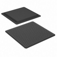
XC3S1500-4FGG676C Xilinx Inc, XC3S1500-4FGG676C Datasheet - Page 94

XC3S1500-4FGG676C
Manufacturer Part Number
XC3S1500-4FGG676C
Description
FPGA Spartan®-3 Family 1.5M Gates 29952 Cells 630MHz 90nm Technology 1.2V 676-Pin FBGA
Manufacturer
Xilinx Inc
Series
Spartan™-3r
Datasheet
1.XC3S50-4VQG100C.pdf
(217 pages)
Specifications of XC3S1500-4FGG676C
Package
676FBGA
Family Name
Spartan®-3
Device Logic Units
29952
Device System Gates
1500000
Maximum Internal Frequency
630 MHz
Typical Operating Supply Voltage
1.2 V
Maximum Number Of User I/os
487
Ram Bits
589824
Number Of Logic Elements/cells
29952
Number Of Labs/clbs
3328
Total Ram Bits
589824
Number Of I /o
487
Number Of Gates
1500000
Voltage - Supply
1.14 V ~ 1.26 V
Mounting Type
Surface Mount
Operating Temperature
0°C ~ 85°C
Package / Case
676-BBGA
Lead Free Status / RoHS Status
Lead free / RoHS Compliant
For Use With
NANO-SPARTAN - KIT NANOBOARD AND SPARTAN3 DC807-1001 - DAUGHTER CARD XILINX SPARTAN 3
Lead Free Status / RoHS Status
Lead free / RoHS Compliant
Other names
122-1337
Available stocks
Company
Part Number
Manufacturer
Quantity
Price
Company:
Part Number:
XC3S1500-4FGG676C
Manufacturer:
XILINX
Quantity:
7
Company:
Part Number:
XC3S1500-4FGG676C
Manufacturer:
XILINX
Quantity:
350
Company:
Part Number:
XC3S1500-4FGG676C
Manufacturer:
XilinxInc
Quantity:
3 000
Company:
Part Number:
XC3S1500-4FGG676C
Manufacturer:
Xilinx Inc
Quantity:
10 000
Part Number:
XC3S1500-4FGG676C
Manufacturer:
XILINX/赛灵思
Quantity:
20 000
Spartan-3 FPGA Family: DC and Switching Characteristics
Table 66: Timing for the Master and Slave Parallel Configuration Modes
94
INIT_B
CS_B
RDWR_B
CCLK
D0 - D7
BUSY
PROG_B
Notes:
1.
Clock-to-Output Times
T
Setup Times
T
T
T
(Input)
(Open-Drain)
(Input)
(Input)
(Input/Output)
(Inputs)
(Output)
SMCKBY
SMDCC
SMCSCC
SMCCW
Symbol
Switching RDWR_B High or Low while holding CS_B Low asynchronously aborts configuration.
(2)
The time from the rising transition on the CCLK pin to a signal
transition at the BUSY pin
The time from the setup of data at the D0-D7 pins to the rising
transition at the CCLK pin
The time from the setup of a logic level at the CS_B pin to the rising
transition at the CCLK pin
The time from the setup of a logic level at the RDWR_B pin to the
rising transition at the CCLK pin
Figure 36: Waveforms for Master and Slave Parallel Configuration
High-Z
T
SMCCW
T
SMDCC
Description
Byte 0
T
SMCSCC
www.xilinx.com
T
SMCCD
Byte 1
T
SMCKBY
T
Master
CCH
Slave/
Slave
Both
BUSY
1/F
DS099-3 (v2.5) December 4, 2009
Byte n
CCPAR
All Speed Grades
T
SMCKBY
10.0
10.0
10.0
Min
-
T
T
CCL
Product Specification
SMCCCS
Byte n+1
Max
12.0
-
-
-
DS099-3_05_041103
T
SMWCC
Units
High-Z
ns
ns
ns
ns
R


