NST3946DXV6T1G ON Semiconductor, NST3946DXV6T1G Datasheet
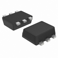
TRANS NPN/PNP 200MA 40V SOT-563

NST3946DXV6T1G

Manufacturer Part Number
NST3946DXV6T1G
Description
TRANS NPN/PNP 200MA 40V SOT-563
Manufacturer
ON Semiconductor
Datasheet

Specifications of NST3946DXV6T1G

Transistor Type
NPN, PNP
Current - Collector (ic) (max)
200mA
Voltage - Collector Emitter Breakdown (max)
40V
Vce Saturation (max) @ Ib, Ic
300mV @ 5mA, 50mA / 400mV @ 5mA, 50mA
Dc Current Gain (hfe) (min) @ Ic, Vce
100 @ 10mA, 1V
Power - Max
500mW
Frequency - Transition
300MHz, 250MHz
Mounting Type
Surface Mount
Package / Case
SOT-563, SOT-6
Lead Free Status / RoHS Status
Lead free / RoHS Compliant
Current - Collector Cutoff (max)
-
Other names
NST3946DXV6T1G
NST3946DXV6T1GOSTR

Available stocks

Company
Part Number
Manufacturer
Quantity
Price
Part Number:
NST3946DXV6T1G
Manufacturer:
ON
Quantity:
30 000
Part Number:
NST3946DXV6T1G
Manufacturer:
ON/安森美
Quantity:
20 000
Company:
Part Number:
NST3946DXV6T1G
Quantity:
5 000
NST3946DXV6T1G,
NST3946DXV6T5G
Dual General Purpose
Transistor
SOT−23/SOT−323 three−leaded device. It is designed for general
purpose amplifier applications and is housed in the SOT−563
six−leaded surface mount package. By putting two discrete devices in
one package, this device is ideal for low−power surface mount
applications where board space is at a premium.
© Semiconductor Components Industries, LLC, 2010
September, 2010 − Rev. 1
MAXIMUM RATINGS
THERMAL CHARACTERISTICS
1. FR−4 @ Minimum Pad
Total Device Dissipation
Derate above 25°C
Thermal Resistance
Total Device Dissipation
Derate above 25°C
Collector −Emitter Voltage
Collector −Base Voltage
Emitter −Base Voltage
Collector Current − Continuous
Electrostatic Discharge
The NST3946DXV6T1 device is a spin−off of our popular
Compliant
h
Low V
Simplifies Circuit Design
Reduces Board Space
Reduces Component Count
These Devices are Pb−Free, Halogen Free/BFR Free and are RoHS
FE
(NPN)
(PNP)
(NPN)
(PNP)
(NPN)
(PNP)
(NPN)
(PNP)
Junction-to-Ambient
, 100−300
(Both Junctions Heated)
(One Junction Heated)
CE(sat)
Characteristic
Characteristic
Rating
, ≤ 0.4 V
T
T
A
A
= 25°C
= 25°C
Symbol
Symbol
Symbol
V
V
V
ESD
R
P
P
CEO
CBO
EBO
I
qJA
C
D
D
HBM>16000,
MM>2000
(Note 1)
(Note 1)
(Note 1)
(Note 1)
(Note 1)
Value
−200
−5.0
Max
Max
−40
−40
200
357
350
500
6.0
2.9
4.0
40
60
1
mW/°C
mW/°C
mAdc
°C/W
Unit
Unit
Unit
Vdc
Vdc
Vdc
mW
mW
V
†For information on tape and reel specifications,
NST3946DXV6T1G SOT−563
NST3946DXV6T5G SOT−563
including part orientation and tape sizes, please
refer to our Tape and Reel Packaging Specification
Brochure, BRD8011/D.
Device
(Note: Microdot may be in either location)
Q
(3)
(4)
1
ORDERING INFORMATION
46 = Specific Device Code
M
G
MARKING DIAGRAM
http://onsemi.com
NST3946DXV6T1*
= Date Code
= Pb−Free Package
CASE 463A
SOT−563
PLASTIC
*Q1 PNP
6
(Pb−Free)
(Pb−Free)
Package
Q2 NPN
(5)
5 4
46 MG
G
(2)
Publication Order Number:
1
2
3
NST3946DXV6T1/D
4000/Tape & Reel
8000/Tape & Reel
Shipping
(1)
(6)
Q
2

Related parts for NST3946DXV6T1G

NST3946DXV6T1G Summary of contents

Page 1

... G = Pb−Free Package (Note: Microdot may be in either location) ORDERING INFORMATION Device Package Shipping NST3946DXV6T1G SOT−563 4000/Tape & Reel (Pb−Free) NST3946DXV6T5G SOT−563 8000/Tape & Reel (Pb−Free) †For information on tape and reel specifications, including part orientation and tape sizes, please refer to our Tape and Reel Packaging Specification Brochure, BRD8011/D ...

Page 2

Characteristic (Both Junctions Heated) Thermal Resistance Junction-to-Ambient Junction and Storage Temperature Range ELECTRICAL CHARACTERISTICS Characteristic OFF CHARACTERISTICS Collector −Emitter Breakdown Voltage (Note 1.0 mAdc −1.0 mAdc ...

Page 3

ELECTRICAL CHARACTERISTICS Characteristic SMALL−SIGNAL CHARACTERISTICS Current −Gain − Bandwidth Product ( mAdc Vdc 100 MHz −10 mAdc −20 Vdc 100 MHz Output Capacitance ...

Page 4

DUTY CYCLE = 2% 300 ns +10 0.5 V < Figure 1. Delay and Rise Time Equivalent Test Circuit TYPICAL TRANSIENT CHARACTERISTICS 10 7.0 5.0 3.0 2.0 1.0 0.1 (NPN < 500 ...

Page 5

1.0 2.0 3.0 5.0 7 COLLECTOR CURRENT (mA) C Figure 4. Turn −On Time 500 ...

Page 6

I , COLLECTOR CURRENT (mA) C Figure 10. Current Gain 20 (NPN) 10 5.0 2.0 1.0 0.5 0.2 0.1 0.2 0.3 0.5 1.0 2 COLLECTOR ...

Page 7

TYPICAL STATIC CHARACTERISTICS 2.0 1.0 0.7 0.5 0.3 0.2 0.1 0.1 0.2 0.3 0.5 0.7 1.0 1 0.6 0.4 0.2 0 0.01 0.02 0.03 0.05 0.07 1.2 (NPN 25° 1.0 ...

Page 8

V 10.6 V 300 ns DUTY CYCLE = 2% Figure 18. Delay and Rise Time Equivalent Test Circuit TYPICAL TRANSIENT CHARACTERISTICS 10 7.0 5.0 3.0 2.0 1.0 0.1 500 (PNP) 300 200 100 70 ...

Page 9

TYPICAL AUDIO SMALL−SIGNAL CHARACTERISTICS (V CE 5.0 SOURCE RESISTANCE = 200 1 4.0 SOURCE RESISTANCE = 200 0 3.0 SOURCE RESISTANCE = 2 2.0 ...

Page 10

TYPICAL STATIC CHARACTERISTICS 2.0 1.0 0.7 0.5 0.3 (PNP) 0.2 0.1 0.1 0.2 0.3 0.5 0.7 1.0 1.0 (PNP 0.6 0.4 0.2 0 0.01 0.02 0.03 0.05 0.07 1 25° ...

Page 11

... M *For additional information on our Pb−Free strategy and soldering details, please download the ON Semiconductor Soldering and Mounting Techniques Reference Manual, SOLDERRM/D. ON Semiconductor and are registered trademarks of Semiconductor Components Industries, LLC (SCILLC). SCILLC reserves the right to make changes without further notice to any products herein ...

Related keywords