AT-64020 Avago Technologies US Inc., AT-64020 Datasheet - Page 2
AT-64020
Manufacturer Part Number
AT-64020
Description
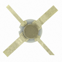
TRANS NPN BIPO 20V 200MA 200-SMD
Manufacturer
Avago Technologies US Inc.
Datasheet
1.AT-64020.pdf
(4 pages)
Specifications of AT-64020
Transistor Type
NPN
Voltage - Collector Emitter Breakdown (max)
20V
Power - Max
3W
Dc Current Gain (hfe) (min) @ Ic, Vce
20 @ 110mA, 8V
Current - Collector (ic) (max)
200mA
Mounting Type
Surface Mount
Package / Case
4-SMD (200 mil BeO)
Transistor Polarity
NPN
Collector Emitter Voltage V(br)ceo
20V
Power Dissipation Pd
3W
Dc Collector Current
200mA
Dc Current Gain Hfe
50
No. Of Pins
4
Peak Reflow Compatible (260 C)
Yes
Number Of Elements
1
Collector-emitter Voltage
20V
Collector-base Voltage
40V
Emitter-base Voltage
2V
Collector Current (dc) (max)
200mA
Dc Current Gain (min)
20
Power Dissipation
3W
Frequency (max)
4GHz
Operating Temp Range
-65C to 200C
Operating Temperature Classification
Military
Mounting
Surface Mount
Pin Count
4
Package Type
BeO
Leaded Process Compatible
Yes
Rohs Compliant
Yes
Lead Free Status / RoHS Status
Lead free / RoHS Compliant
Gain
-
Frequency - Transition
-
Noise Figure (db Typ @ F)
-
Lead Free Status / Rohs Status
Compliant
Other names
516-1861
AT-64020
AT-64020
Available stocks
Company
Part Number
Manufacturer
Quantity
Price
Company:

Part Number:
AT-64020
Manufacturer:
SYNERGY
Quantity:
5 000
Part Number:
AT-64020
Manufacturer:
AGILENT
Quantity:
20 000
Company:
Part Number:
AT-64020-TR1
Manufacturer:
FREESCALE
Quantity:
120


AT-64020 Absolute Maximum Ratings
Electrical Specifications, T
Note:
1. ηT = (RF Output Power)/(RF Input Power + VCEIC).
Symbol
|S
P
G
η
h
I
I
CBO
EBO
1 dB
T
FE
1 dB
1E
Symbol
V
V
V
T
|
P
EBO
CBO
CEO
I
T
STG
C
T
j
Insertion Power Gain; V
Power Output @ 1 dB Gain Compression
V
1 dB Compressed Gain; V
Total Efficiency at 1 dB Compression:
V
Forward Current Transfer Ratio; V
Collector Cutoff Current; V
Emitter Cutoff Current; V
CE
CE
= 16 V, I
= 16 V, I
Parameter
Emitter-Base Voltage
Collector-Base Voltage
Collector-Emitter Voltage
Collector Current
Power Dissipation
Junction Temperature
Storage Temperature
C
C
= 110 mA
= 110 mA
Parameters and Test Conditions
A
= 25°C
CE
EB
CE
CB
= 16 V, I
= 16 V, I
= 1 V
= 16 V
[,3]
CE
C
= 8 V, I
C
= 110 mA
= 110 mA
C
= 110 mA
[1]
Units
mA
W
°C
°C
V
V
V
f = .0 GHz
f = 4.0 GHz
f = .0 GHz
f= 4.0 GHz
f = .0 GHz
f = 4.0 GHz
f = 4.0 GHz
Maximum
-65 to 00
Absolute
00
00
40
0
3
[1]
Units
dBm
—
dB
dB
µA
µA
%
Thermal Resistance
Notes:
1. Permanent damage may occur if any of
2. Tcase = 25°C.
3. Derate at 25 mW/°C for Tc > 80°C.
4. The small spot size of this technique results
θ
jc
these limits are exceeded.
in a higher, though more accurate determi-
nation of θjc than do alternate methods.
See MEASUREMENTS section “Thermal Re-
sistance” for more information.
= 40°C/W
Min.
6.5
8.5
0
[2,4]
:
7.5
6.5
10.0
35.0
Typ.
7.0
.0
6.5
50
Max.
00
100
5.0
Related parts for AT-64020
Image
Part Number
Description
Manufacturer
Datasheet
Request
R

Part Number:
Description:
TRANS NPN BIPO 12V 80MA 35-SMD
Manufacturer:
Avago Technologies US Inc.
Datasheet:

Part Number:
Description:
IC TRANS NPN BIPOLAR SOT-23
Manufacturer:
Avago Technologies US Inc.
Datasheet:

Part Number:
Description:
IC TRANS NPN BIPOLAR SOT-363
Manufacturer:
Avago Technologies US Inc.
Datasheet:

Part Number:
Description:
TRANS NPN BIPO 5.5V 16MA SOT-23
Manufacturer:
Avago Technologies US Inc.
Datasheet:

Part Number:
Description:
IC TRANS NPN BIPOLAR SOT-143
Manufacturer:
Avago Technologies US Inc.
Datasheet:

Part Number:
Description:
TRANS SIL LOW NOISE BIPOL 45MD
Manufacturer:
Avago Technologies US Inc.
Datasheet:

Part Number:
Description:
TRANS NPN BIPO 12V 80MA 86-SMD
Manufacturer:
Avago Technologies US Inc.
Datasheet:

Part Number:
Description:
TRANS NPN BIPO 12V 60MA 35-SMD
Manufacturer:
Avago Technologies US Inc.
Datasheet:

Part Number:
Description:
TRANS NPN BIPO 12V 80MA 86-SMD
Manufacturer:
Avago Technologies US Inc.
Datasheet:

Part Number:
Description:
RF TRANSISTOR, NPN, 12V, 8GHZ 85 PLASTIC
Manufacturer:
Avago Technologies US Inc.
Datasheet:
Part Number:
Description:
IC TRANS NPN BIPOLAR SOT-23
Manufacturer:
Avago Technologies US Inc.
Datasheet:
Part Number:
Description:
IC TRANS NPN BIPOLAR SOT-363
Manufacturer:
Avago Technologies US Inc.
Datasheet:
Part Number:
Description:
TRANS NPN BIPO 5.5V 16MA SOT-23
Manufacturer:
Avago Technologies US Inc.
Datasheet:
Part Number:
Description:
IC TRANS NPN BIPOLAR SOT-143
Manufacturer:
Avago Technologies US Inc.
Datasheet:
Part Number:
Description:
BJT (Bipolar Junction Transistor)
Manufacturer:
Avago Technologies US Inc.